The MARIE: A
Simple Computer
Goals for this chapter:
1. Describe the top–level organization of a
modern stored–program computer;
specifically name and describe
the four main components.
2. Describe some of the lower–level components,
such as registers,
that are common to three of the
four main components of the computer.
3. Define an assembly language for this simple
computer and use that assembly
language to investigate the
functioning of a stored program computer.
NOTES:
1. The hypothetical computer designed by our
textbook’s authors is called
the MARIE. See the textbook for the origin of the name.
2. The MARIE has an extremely simple
design. Any computer the student sees or
uses, including the computers in
one’s microwave oven and washing machine,
are more powerful than the
MARIE.
3. While a very simple design, the MARIE
illustrates all of the important features
of a modern stored–program
computer. “Simpler” means “easier to
learn”.
Why a Binary
Computer?
The MARIE is typical of all modern computers in that
it is a binary device.
1. All data are stored in binary format, and
2. All arithmetic is performed using
two’s–complement binary conventions.
Why not have decimal format? Just create memory elements that store one of
10 values.
The answer has two parts. Each is valid.
1. It is easy to make binary storage devices and
binary arithmetic devices.
2. There are a number of significant design
challenges in creating ten–state
devices. Mostly these have to do with electronic reliability.
In fact, no modern electronic computer has ever used
true decimal storage and arithmetic.
Early machines, such as the ENIAC, were called decimal
computers. In fact:
1. Each decimal digit was stored in binary
format, and
2. All arithmetic was done in binary format, as
adapted for storage
of individual decimal digits.
Computer
Basics and Organization
The computer has four top–level components.
1. The
CPU (Central Processing Unit)
2. The
Main Memory
3. Input/Output
Devices, including a Hard Disk
4. A
Bus Structure to facilitate communications between the other components.

Major
Components Defined
The system
memory (of which this computer has 512 MB) is used for transient storage of
programs and data. This is accessed much
like an array, with the memory address
serving the function of an array index.
The Input /
Output system (I/O System) is used for the computer to save data and
programs and for it to accept input data and communicate output data.
Technically the hard drive is an I/O
device.
The Central
Processing Unit (CPU) handles execution of the program.
It has four main components:
1. The
ALU (Arithmetic Logic Unit), which
performs all of the arithmetic
and logical operations of the
CPU, including logic tests for branching.
2. The
Control Unit, which causes the CPU
to follow the instructions
found in the assembly language
program being executed.
3. The
register file, which stores data internally in the CPU. There are user
registers and special purpose
registers used by the Control Unit.
4. A
set of internal busses to allow the CPU units to communicate.
A
System Level Bus, which allows the
top–level components to communicate.
The System
Clock
We discussed the system clock when we discussed the basic
flip–flops.
Here are two depictions of the system clock that will
be used in this course.
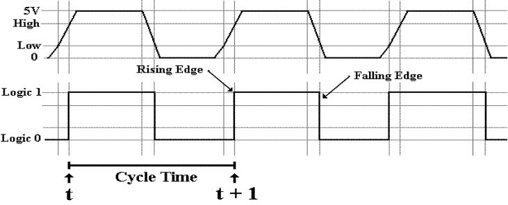
The top representation is used when discussing the
system bus and the I/O bus.
The bottom representation is used elsewhere.
The
system clock regulates the execution of instructions in the CPU and
synchronizes all of the CPU components to prevent errors due to bad timing.
The System Bus
The system bus
comprises a set of digital lines; each of which carries a signal, power, or
ground. The ground is used to complete
circuits.
If the line carries a signal, that line is set either
to logic 1 (often +5 volts) or logic 0
(often 0 volts). Consider it as
transmitting a Boolean variable, in that the value on
that line can be changed by some control unit as a program is executed.
The ground lines also provide isolation between the
signal lines, which can act as little antennas – either to “broadcast” signals
or receive them from other signal lines.
This is called “cross talk”. It is not
desirable.
High–speed busses are shorter than low–speed
busses. High–speed busses are used for:
1. Connecting
the CPU to main memory,
2. Connecting
the CPU to the graphics system, and
3. Possibly
connecting the CPU to other high–speed devices.
Low–speed busses are used to connect the CPU to I/O
devices, possibly including the
main hard disk.
The
speed of a data bus is determined by the time it takes an electrical signal to
travel its
length. Light travels about 1 foot per
nanosecond; signals travel about 8 inches in that time. A bus operating at 1 GHz cannot be longer
than 8 inches; likely it is shorter.
Notations
Used for a Bus
Here is the way that we would commonly represent a
small bus.
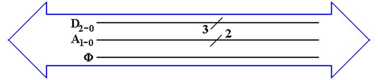
The big “double arrow” notation indicates a bus of a number of
different signals.
Our author calls this a “fat arrow”.
Lines with similar function are grouped together. Their count is denoted with the
“diagonal slash” notation.
From top to bottom, we have
1. Three
data lines D2,
D1, and D0
2. Two address lines A1 and A0
3. The clock signal for the bus F.
Not all busses transmit a clock
signal; the system bus does.
Power and ground lines usually are not shown in this
diagram.
Busses:
Common and Point–to–Point
In general, a design should minimize point–to–point
busses, as they introduce a
number of difficulties into the design.
Shared busses tend to have lower data rates than
point–to–point busses, which then
are the design choice when the bus must support a high data rate.
Typical high–rate busses include the memory bus and
the graphics bus. Each of these
is implemented as a point–to–point bus for two reasons:
1. To
maximize the data rate, and
2. Because
there is only one device with which the CPU communicates.
Some high–rate busses are shared busses. An example would be a bus connecting the
ALU to the register file in the CPU. At
any time, at most one of the registers is using
this bus to communicate data to the ALU.
Busses that manage most I/O devices tend to be shared.
Connecting
External Devices to the Computer Bus
External devices include printers, network cards, disk
drives, and the computer keyboard.
Each device must be connected to one of the computer
busses through a device called
an interface, often an “interface card”.
Each device will have software dedicated to controlling
it, called a “device driver”.
Device drivers are often considered part of the
computer operating system, because
they are called only by the operating system.
The main function of the device driver is to translate
between the standard device
control signals used by the operating system and the device–specific control
signals required by the device’s interface card.
The function of the interface card is to present the
data and control signals, properly
formatted, to the device being managed, and accept data back.
From the view of the CPU, each device is represented
as a number of addressable
registers, some containing data and some control information. The interface card
presents these to the actual device. We
shall develop this idea later.
Asynchronous
and Synchronous Busses
One aspect of a bus depends on what assumptions can be
made about the timing of
the devices attached. Can each device be
assumed to work with fixed timing?
Consider a keyboard attached to a common bus. This produces data only when a
user actually presses a key. The timing
of data availability is totally unpredictable.
In cases such as managing most I/O devices, an asynchronous bus is used. This means
that there is no clock signal used to coordinate events.
An asynchronous bus must use specific control signals
to coordinate between the device
producing the data and the device receiving the data. Here is a sample set:
Request the CPU signals the device that input is
required.
Ready the input device signals the CPU that
data are ready to be read.
ACK the CPU acknowledges that it has
received the data.
For some devices, such as memory, we may assume
constant timings. Here we have
fewer control signals. The sequence to
read memory is typically simple.
1. The CPU asserts a memory address and the READ
control signal.
2. After a fixed time, the CPU reads the data
from the appropriate memory register.
The data can be assumed to be
present and correct at the specified time.
The Memory
Component
The memory stores the instructions and data for an
executing program.
Memory is characterized by the smallest addressable
unit:
Byte addressable the smallest unit is an 8–bit byte.
Word addressable the smallest unit is a word, usually 16
or 32 bits in length.
Most modern computers are byte addressable,
facilitating access to character data.
Logically, computer memory should be considered as an
array.
The index into this array is called the address or “memory address”.
A logical view of such a byte addressable memory might
be written in code as:
Const MemSize =
byte Memory[MemSize] // Indexed 0 … (MemSize – 1)
The CPU has two registers dedicated to handling
memory.
The MAR (Memory Address Register) holds the
address being accessed.
The MBR (Memory Buffer Register) holds the data
being written to the
memory or
being read from the memory. This is
sometimes
called the
Memory Data Register.
The
Simplistic Physical View of Memory
I call this the “linear view”, as memory is still
modeled as one large linear array.
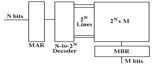
The N–bit address selects one of the 2N entities,
numbered 0 through (2N – 1).
Read sequence: First address
to MAR; command a READ.
then copy the contents of the MBR.
Write sequence: First address
to MAR; data to the MBR.
then command a WRITE.
This is logically correct, but difficult to implement
at an acceptable price.
Memory
Organization and Addressing
Memory
is based on binary bits. Each bit can
hold one of two values: 0 or 1.
Except
for unusual designs, individual bits in memory are not directly addressable
by the CPU (Central Processing Unit).
The old IBM 1401 could access bits directly.
The
most common memory groupings are as follows:
8 bits a byte
16 bits a word (some
call this a short word)
32 bits a longword (some
call this a word)
The
term “word” is somewhat ambiguous due to multiple definitions. In this course, we refer to “16–bit word”,
“32–bit word”, etc.
In
some computers, a word is the smallest addressable memory unit. Most of these, such as the CDC–6600 (60–bit
words) are now obsolete.
In
a byte–addressable computer (such as the Intel Pentium series), each byte is
addressable individually, although 32–bit words can be directly accessed.
All
computers with byte addressing provide instructions to access both 16–bit words
and
32–bit longwords. The CPU just accesses
two or four bytes at a time.
Memory
Organization and Addressing (Part 2)
Memory
is often described by a notation with the structure (L x W)
L is the number of addressable units in
memory
W is the number of bits in memory
The
old CDC–6600 usually had a 256 K x 60 memory.
This was 256 · 1024 =
262, 144 words, each of 60 bits. Yes,
this was called a “supercomputer”.
A
modern Pentium might have a memory described as 512 M x 8;
512 · 220 = 512 · 1, 048, 576 = 536,870,912 addressable units, each
with 8 bits.
This would be called a 512 MB
memory.
Main
memory sizes are not quoted in bits.
Memory chip sizes often are quoted in bits,
but could be quoted in numbers of 4–bit elements as well as 8–bit bytes.
Common
notation: 1K = 210 = 1, 024 (almost never seen these
days)
1M = 220
= 1, 048, 576
1G = 230
= 1, 073, 741, 824
Address
Space and Memory Addressing
N
bits will address 2N items.
Pentium has 32 bit addressing and will address 232 bytes.
To
address M items, we need N bits, with 2N–1 < M £ 2N.
Quite often these days, we
have either M = 2N (obviously requiring N bits to address). It is also the case that we normally just
state the number of address bits and keep the actual memory small enough.
Example: One of my
recent laptop computers had 384 MB of byte–addressable
memory. How many bits would be required to address
this?
Answer: This memory has 384 MB as is byte addressable, so it
has to be able
to address 384·220 distinct memory cells. 1M = 220 = 1, 048, 576.
Now 384 = 256 + 128 = 28
+ 27,
so 384 MB = 384·220 bytes = (28 + 27)·220 bytes = (228 + 227)
bytes.
If
M = (228 + 227), it should be obvious that 228
< M £ 229, so we
need a 29–bit address.
Practicality: All Pentium
computers provide a 32–bit address through
a 32–bit MAR (Memory Address Register).
RULE: Memory is cheap. You can never have enough memory on a
computer.
When you buy a computer,
buy all the memory it can be configured to use.
Memory as a
Collection of Chips
In
fact, physical memory is built from standard memory chips. For example, a 256 MB memory might be built
from sixteen 16 MB chips, each of which might itself be implemented as eight 16
Mb (megabit) chips; a total of 128 chips.
Consider
the textbook’s example: a 32 KB memory built from 4KB chips.
32
KB = 215 bytes and 4 KB = 212 bytes. We need (215 / 212) = 23
= 8 chips. In standard fashion, these
chips will be numbered as 0 through 7 inclusive.
We
need a 15–bit address for this memory.
Address bits are numbered 14 through 0.
Here
we adopt low order interleaving. Consecutive addresses are placed in different
chips. This facilitates faster access to
memory. Here is the textbooks figure
showing the location of the first 32 addressable bytes.
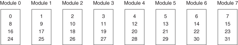
Low–Order
Interleaving: Partitioning the Address
Low–order
interleaving will always use a chip count that is a power of 2; 2K
with K > 1.
The
N–bit memory address will be broken into K bits for the chip selection and
(N – K) address bits for each
chip.
In
our example N = 15 and K = 3. In this
low–order interleaving, the three low order bits select the chip to be
used. These are bits 2, 1, and 0.
|
bit |
14 |
13 |
12 |
11 |
10 |
9 |
8 |
7 |
6 |
5 |
4 |
3 |
2 |
1 |
0 |
|
|
12–bit address to each chip. |
Chip Select |
|||||||||||||
In high–order
interleaving (also called “memory banking”, not much used)
the high–order K bits select the
chip. In our example
bits 14 – 12 select the chip and
bits 11 – 0 are sent to each chip.
In low–order
interleaving Chip_Number = Address Mod 2K, the remainder from
division by the number of chips in the chip set. Always this count is a power of 2.
This organization is often
closely connected to the size of the memory cache blocks.
If the memory is 2K–way interleaved (low order), each cache line might
have 2K bytes.
Why have
low–order interleaving?
This
choice is due to the principle of locality; memory locations tend to be
accessed one after another. If
consecutive locations are in different chips, the CPU can initiate a number of
memory–read operations at a rate faster than the memory chips can handle.
Consider
the organization from the book, with an 8–way low interleaving.
Suppose
that the CPU wants to fill a cache line with the eight bytes, indexed 8 to 15.
The
CPU sends an address and READ command to module 0.
Without waiting for a response, the CPU sends an address and READ to module 1.
Finally,
the CPU sends an address and READ command to module 7.
Then,
the CPU actually reads from module 0.
If the memory access time is 80 nanoseconds, the CPU can issue on command every
10 nanoseconds as it will take 80 nanoseconds to get back and read a given
module.
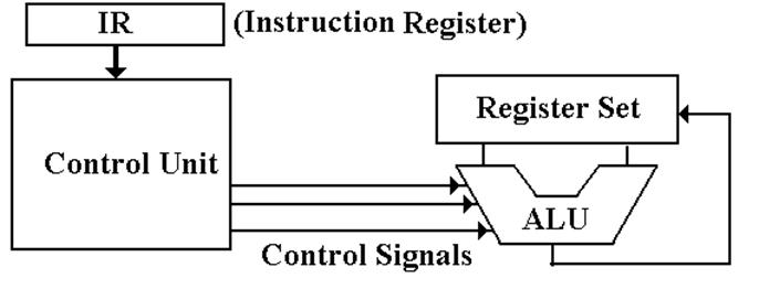
The Central
Processing Unit (CPU)
The CPU also has four main components:
1. The
Control Unit (along with the IR) interprets the machine language instruction
and issues the control signals to
make the CPU execute it.
2. The
ALU (Arithmetic Logic Unit) that does the arithmetic and logic.
3. The
Register Set (Register File) that stores temporary results related to the
computations. There are also Special Purpose Registers used by the Control Unit.
4. An
internal bus structure for communication.
The Register
File
There are two sets of registers, called “General
Purpose” and “Special Purpose”.
The origin of the register set is simply the need to
have some sort of memory on the computer and the inability to build what we now
call “main memory”.
When reliable technologies, such as magnetic cores,
became available for main memory, the concept of CPU registers was retained.
Registers are now implemented as a set of flip–flops
physically located on the CPU chip.
These are used because access times for registers are two orders of
magnitude faster than access times for main memory: 1 nanosecond vs. 80
nanoseconds.
General
Purpose Registers
These are mostly used to store intermediate results of computation. The count of such registers is often a power
of 2, say 24 = 16 or 25 = 32, because N bits address 2N
items.
The registers are often numbered and named with a
strange notation so that the assembler will not confuse them for variables;
e.g. %R0 … %R15. %R0 is often fixed at
0.
NOTE: The MARIE has
only one general purpose register – the AC (Accumulator).
Think of the AC as the
display on a standard calculator.
The Register
File
Special
Purpose Registers
These are often used by the control
unit in its execution of the program.
PC the Program
Counter, so called because it does not count anything.
It is also called the IP (Instruction Pointer), a much better
name.
The PC points to the
memory location of the instruction to be executed next.
IR the Instruction
Register. This holds the machine
language version of
the instruction currently
being executed.
MAR the Memory
Address Register. This holds the
address of the memory word
being referenced. All execution steps begin with PC ® MAR.
MBR the Memory
Buffer Register, also called MDR (Memory Data Register).
This holds the data being
read from memory or written to memory.
PSR the Program
Status Register, often called the PSW (Program Status Word),
contains a collection of
logical bits that characterize the status of the program
execution: the last result
was negative, the last result was zero, etc.
SP on machines that use a stack
architecture, this is the Stack Pointer.
Connecting a
D Flip–Flop to a Data Bus
Registers are normally implemented with D flip–flops,
one for each bit stored.
Cache memory can be considered to be fabricated from D
flip–flops. Being made
with a technology called “SRAM” (defined later), this might even be true.
Main memory can be considered to be fabricated from D
flip–flops, but it is not.
Here the idea is just a good logical model.
There needs to be a way to place a number of D
flip–flops on a pair of common data
busses so that each flip–flop can be written to and read from.
To avoid naming problems, I call the two data busses
“To Register” and “From Register”.
Suppose a register file with 32 registers, numbered 0
through 31. Each register in the
file stores 16 bits. Thus, each of the
two data busses must have 16 data lines.
We have two questions to consider at this point.
1. How
to connect a D flip–flop to the “To Register” data line so that it is loaded
with data only when it is
supposed to be, and
2. How to connect a D flip–flop to the “From
Register” data line so that it outputs
data only when it is supposed to
output.
Controlling
Input to a D Flip–Flop
A D flip–flop copies the value on the D input on every
rising clock edge.
It is not possible to shut down the D input, it always has a value.
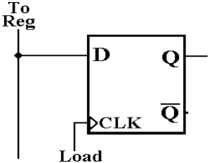
The only way to control input to the flip–flop is
through use of the CLK input signal,
which is here shown connected to a control called “Load”.
When Load = 0, the flip–flop does not respond to input
and retains its value.
When Load is pulsed from 0 to 1, the flip–flop will
load whatever value is on the
bus line “To Reg”.
More on
Input to a D Flip–Flop
The control signal Load must be synchronized with the
system clock.
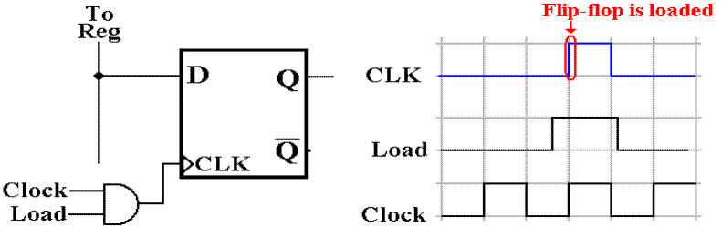
The Load signal for this flip–flop is generated by the
Control Unit to arrive just before
the rising edge of the system clock, allowing a valid CLK input signal to be
generated.
There is a load signal for each register in the
register file. Each flip–flop in the
register
receives the same Load signal and loads at the same time.
Two One–Bit
Registers
This two–register set shows how to select the register
to be loaded.

When L0 is pulsed, the top register is
loaded.
When L1 is pulsed, the bottom register is
loaded.
When neither is pulsed, each register keeps its
contents.
Theoretically, one might pulse both L0 and
L1. In practice, this is
seldom done.
Managing
Flip–Flop Output: the Tri–State Buffer
We now need a simple way to connect the output of the
flip–flop to the “From
Register” bus. This is the output
labeled as Q. The best choice is a tri–state buffer.
The tri–state buffer is just an automatic switch that
can be turned on and off.
Here are the diagrams for two of the four most popular
tri–state buffers.
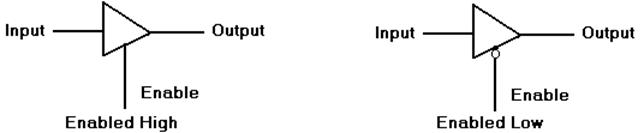
What does the tri–state do when it is enabled?
What does the tri–state do when it is not enabled?
We shall focus on the enabled–high tri–state
buffer. The other is similar.
An
Enabled–High Tri–State Buffer
Consider
an enabled–high tri–state buffer, with the enable signal called “C”.
When C = 1, the buffer is enabled.
When C = 0, the buffer is not
enabled.
What
does the buffer do?
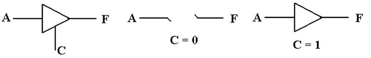
The
buffer should be considered a switch.
When C = 0, there is no connection between the input A and the output
F. When C = 1, the output F is connected
to the input A via what appears to be a non–inverting buffer.
Strictly
speaking, when C = 0 the output F remains connected to input A, but through a
circuit that offers very high resistance to the flow of electricity. For this reason, the state is often called “high impedance”, “impedance” being an
engineer’s word for “resistance”.
Sample Use
of Tri–State Buffers
Here
is a circuit that uses a pair of tri–state buffers to connect exactly
one of two inputs to an output. The
effect of the circuit is at right.

Here
is the equivalent circuit using the standard gates.

Connecting
the Flip–Flop Output to a Bus
Each flip–flop in a register file can be connected to
a bit line in the “From Register”
bus using a tri–state buffer.
When Read = 0, the Q output is not connected to the
bus line “From Reg” and
nothing is output to that bus.
When Read = 1, the Q output becomes connected to the
bus line “From Reg” on the
next rising edge of the clock. The
flip–flop value is output to the bus.
The control unit of the CPU must insure proper timing
of the Read control signal.
Registers
and D Flip–Flops
Registers are often built from D flip–flops. A 16–bit register has 16 D flip–flops.
Here is a diagram of a single 2–bit register to show
how the flip–flops are used.
There are two 2–bit busses, one carrying data to the registers and one data
from them.
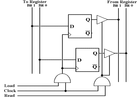
When Clock = 1 and Load = 1, the register accepts
input from the “To Register” bus.
When Clock = 1 and Read = 1, the register puts data
onto the “From Register” bus.
The ALU
(Arithmetic Logic Unit)
The ALU performs all of the arithmetic and logical
operations for the CPU.
These include the following:
Arithmetic: addition, subtraction, negation, etc.
Logical: AND, OR, NOT, Exclusive OR, etc.
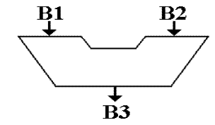
This symbol has been used for the ALU since the mid
1950’s.
It shows two inputs and one output.
The reason for two inputs is the fact that many
operations, such as addition and logical AND, are dyadic; that is, they take two input arguments.
The
Fetch–Execute Cycle
This cycle is the logical basis of all stored program computers.
Instructions are stored in memory as machine language.
Instructions are fetched
from memory and then executed.
The common fetch cycle can be expressed in the
following control sequence.
MAR ¬ PC. //
The PC contains the address of the instruction.
READ. // Put the address into the
MAR and read memory.
IR ¬ MBR. //
Place the instruction into the MBR.
This cycle is described in many different ways, most
of which serve to highlight additional steps required to execute the
instruction. Examples of additional
steps are: Decode the Instruction, Fetch the Arguments, Store the Result, etc.
A stored program computer is often called a “von
Neumann Machine” after one of the originators of the EDVAC.
This Fetch–Execute cycle is often called the “von Neumann bottleneck”, as the
necessity for fetching every instruction from memory slows the computer.
Input/Output
System
Each I/O device is connected to the system bus through
a number of registers.
Collectively, these form part of the device
interface.
These fall into three classes:
Data Contains data to be written to the
device or just read from it.
Control Allows the CPU to control the
device. For example, the CPU
` might instruct a printer to insert a CR/LF after each line
printed.
Status Allows the CPU to monitor the status
of the device. For example
a printer might
have a bit that is set when it is out of paper.
There are two major strategies for interfacing I/O
devices.
Memory Mapped I/O
is designated through specific addresses
Load KBD_Data This would be an input, loading into the
AC
Store LP_Data This would be an output, storing into
a special address
Isolated I/O (Instruction–Based I/O) Uses special instructions.
Input Read from the designated Input Device
Output Write
to the designated Output Device
Interrupts
Efficient
management of Input / Output devices demands that these devices be able to
signal the CPU when they are ready to initiate a data transfer.
For
an input device, this occurs when new data are in its input buffer.
For
an output device, this occurs when the device buffer is empty and the device
can accept new data for later
output.
While
easier to understand within an I/O context, interrupts can occur in other
contexts.
1. Errors
and malfunctions.
2. Page
faults in a virtual memory system (these are hard to handle).
3. Software
interrupts or “traps” that allow user software to signal the
Operating System. These differ slightly from standard procedure
calls.
Interrupts
are either maskable (that is, the
CPU can be set to ignore them) or nonmaskable. Generally, the only reason to mask interrupts
occurs during that small time of program execution in which the CPU is
beginning to process an interrupt.
Improper
masking of interrupts can cause a system to crash.