The Memory
Component
The memory stores the instructions and data for an
executing program.
Memory is characterized by the smallest addressable
unit:
Byte
addressable the smallest unit is
an 8–bit byte.
Word
addressable the smallest unit is a
word, usually 16 or 32 bits in length.
Most modern computers are byte addressable,
facilitating access to character data.
Logically, computer memory should be considered as an
array.
The index into this array is called the address
or “memory address”.
A logical view of such a byte addressable memory might
be written in code as:
Const MemSize =
byte Memory[MemSize] // Indexed 0 … (MemSize
– 1)
The CPU has two registers dedicated to handling
memory.
The MAR (Memory Address Register) holds the
address being accessed.
The MBR (Memory Buffer Register) holds the data being written to the
memory or
being read from the memory. This is
sometimes
called the
Memory Data Register.
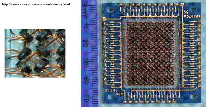
Primary
Memory
Also
called “core memory”, “store”, or “storage”.
Beginning
with the MIT Whirlwind and continuing for about 30 years, the
basic technology for primary memory involved “cores” of magnetic material.
Requirements
for a Memory Device
1. Random access by address, similar to use of
an array. Byte addressable
memory can be considered as an
array of bytes.
byte memory [N] // Address ranges from 0 to (N –
1)
2. Binary memory devices require two reliable
stable states.
3. The transitions between the two stable
states must occur quickly.
4. The transitions between the two stable
states must not occur
spontaneously, but only in response
to the proper control signals.
5. Each memory device must be physically small,
so that a large number
may be placed on a single memory
chip.
6. Each memory device must be relatively inexpensive
to fabricate.
Varieties of
Random Access Memory
There
are two types of RAM
1. RAM read/write memory
2. ROM read–only memory.
The
double use of the term “RAM” is just accepted.
Would you say “RWM”?
Types
of ROM
1. “Plain
ROM” the contents of the memory are
set at manufacture
and
cannot be changed without destroying the chip.
2. PROM the contents of the chip are set
by a special device
called
a “PROM Programmer”. Once programmed
the
contents are fixed.
3. EPROM same as a PROM, but that the
contents can be erased
and
reprogrammed by the PROM Programmer.
Memory
Registers
MAR Memory Address Register
This specifies the address
of the instruction or data item.
For
a byte addressable memory, each byte has a distinct address.
For a word addressable memory, only the words have individual addresses.
MBR Memory Buffer Register
This holds the data read
from memory or to be written to memory.
Occasionally called MDR for
Memory Data Register
In
a byte addressable memory, the MBR is usually 8 bits wide; that is, it
holds one byte.
In
a 16–bit word addressable memory, the MBR would be 16 bits wide.
The
size of the MBR is the size of an addressable item.
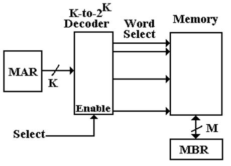
Memory
Control Signals
Read
/ Write Memory must do three actions:
READ copy
contents of an addressed word into the MBR
WRITE copy
contents of the MBR into an addressed word
NOTHING the
memory is expected to retain the contents written into
it until those
contents have been rewritten.
One
set of control signals Select – the memory unit is selected.
![]() if 0 the CPU writes
to memory, if 1 the CPU reads from memory.
if 0 the CPU writes
to memory, if 1 the CPU reads from memory.
|
Select |
|
Action |
|
0 |
0 |
Memory contents are not
changed. |
|
0 |
1 |
Memory contents are not
changed. |
|
1 |
0 |
CPU writes data to the
memory. |
|
1 |
1 |
CPU reads data from the
memory. |
A ROM has only one control
signal: Select.
If
Select = 1 for a ROM, the CPU reads data from the addressed memory slot.
Memory
Timings
Memory Access Time
Defined
in terms of reading from memory. It is
the time between the address
becoming stable in the MAR and the data becoming available in the MBR.
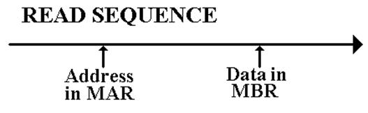
Memory Cycle Time
Less
used, this is defined as the minimum time between two independent
memory accesses.
The Idea of
an Address Space
The
memory size is defined in terms of
the amount of primary memory
actually installed.
The
address space, determined by the
size of the MAR, indicates the range
of addresses that actually can be generated.
Absent
such kludges such as Expanded Memory and Extended Memory
(both obsolete, dating to about 1980), the memory size does not exceed
the size of the address space.
An
N–bit MAR can address 2N distinct memory locations, 0 … 2N
– 1
|
Computer |
MAR bits |
|
|
PDP-11/20 |
16 |
0 to
65 535 |
|
Intel 8086 |
20 |
0 to 1 048 575 |
|
Intel Pentium |
32 |
0 to 4 294 967 295 |
Memory
Mapped Input / Output
Though
not a memory issue, we now address the idea of memory mapped
input and output. In this scheme, we
take part of the address space that
would otherwise be allocated to memory and allocate it to I/O devices.
The
PDP–11 is a good example of a memory mapped device. It was a
byte addressable device, meaning that each byte had a unique address.
The
old PDP–11/20 supported a 16–bit address space.
This supported
addresses in the range 0 through 65,535 or 0 through 0177777 in octal.
Addresses
0 though 61,439 were reserved for physical memory.
In octal these addresses are given by 0 through 167,777.
Addresses
61,440 through 65,535 (octal 170,000 through 177,777)
were reserved for registers associated with Input/Output devices.
Examples: CR11 Card Reader 177,160 Control
& Status Register
177,162 Data buffer 1
177,164 Data buffer 2
The Linear View of Memory
Memory
may be viewed as a linear array, for example a byte–addressable memory
byte memory [N] ; //
Addresses 0 .. (N – 1)
This
is a perfectly good logical view, it just does not correspond to reality.
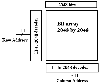
Memory Chip
Organization
Consider
a 4 Megabit memory chip, in which each bit is directly addressable.
Recall that 4M = 222 = 211 · 211, and that 211 = 2, 048.
The
linear view of memory, on the previous slide, calls for a 22–to–222
decoder,
also called a 22–to–4,194,304 decoder. This is not feasible.
If
we organize the memory as a two–dimensional grid of bits, then the design
calls for two 11–to–2048
decoders. This is still a stretch.
Managing
Pin-Outs
Consider
now the two–dimensional memory mentioned above.
What pins are needed?
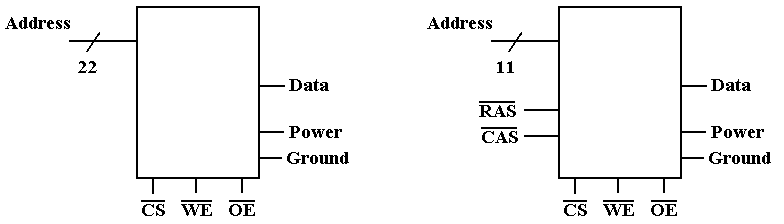
Pin Count
Address Lines 22 Address
Lines 11
Row/Column 0 Row/Column 2
Power & Ground 2 Power
& Ground 2
Data 1 Data 1
Control 3 Control 3
Total 28 Total 19
Separate row and column addresses require two cycles
to specify the address.
Four–Megabyte
Memory
Do
we have a single four–megabyte chip or eight four–megabit memory chips?
One
common solution is to have bit–oriented chips.
This facilitates the
two–dimensional addressing discussed above.
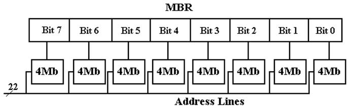
For
applications in which data integrity is especially important, one might add a
ninth chip to hold the parity bit. This reflects the experience that faults,
when they
occur, will be localized in one chip.
Parity
provides a mechanism to detect, but not correct, single bit errors.
Correction
of single bit errors requires twelve memory chips. This scheme will
also detect all two–bit errors.
Memory
Interleaving
Suppose
a 64MB memory made up of the 4Mb chips discussed above.
We now ignore parity memory, for convenience and also because it is rarely
needed.
We
organize the memory into 4MB banks, each having eight of the 4MB chips.
The figure in the slide above shows such
a bank.
The
memory thus has 16 banks, each of 4MB.
16 =
24 4 bits to
select the bank
4M = 222 22 bits address to each chip
Not
surprisingly, 64M = 226.
In
general, an N–bit address, with N = L + M, is broken into two parts
an L–bit bank select, used to activate
one of the 2L banks of memory, and
an M–bit address that is sent to each of
the memory banks.
When
one of the memory banks is active, the other (2L – 1) are inactive.
All
banks receive the M–bit address, but the inactive ones do not respond to it.
High–Order
Interleaving (Memory Banking)
In high-order
interleaving, the most significant bits of the address select the
memory chip. The low–order bits are sent
as addresses to each chip.
|
Bits |
25 – 22 |
21 – 0 |
|
Use |
Bank Select |
Address to the chip |
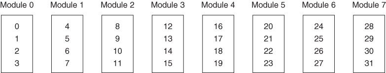
This
idea is intuitively appealing, but suffers from performance penalties.
One
problem is that consecutive addresses tend to be in the same chip.
The
maximum rate of data transfer is set by the memory cycle time,
usually about 50 to 80 nanoseconds.
Low–Order
Interleaving
In
low–order interleaving, the least significant bits select the memory bank
(module).
|
Bits |
25 – 4 |
3 – 0 |
|
Use |
Address to the chip |
Bank Select |
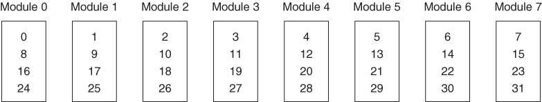
Notice
that consecutive memory addresses are in different memory modules.
This
allows memory access at much faster rates that allowed by the cycle time.
Faster
Memory Chips
We
can use the “2 dimensional” array approach, discussed earlier, to create a
faster
memory. This is done by adding a SRAM
(Static RAM) buffer onto the chip.
Consider the 4Mb (four megabit) chip
discussed earlier, now with a 2Kb SRAM buffer.
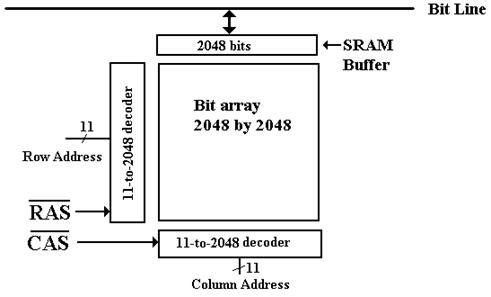
In a modern scenario for reading the chip, a Row
Address is passed to the chip,
followed by a number of column
addresses. When the row address is
received,
the entire row is copied into the SRAM
buffer. Subsequent column reads come
from that buffer.
Memory
Technologies: SRAM and DRAM
One
major classification of computer memory is into two technologies
SRAM Static
Random Access Memory
DRAM Dynamic
Random Access Memory (and its variants)
SRAM
is called static because it will
keep its contents as long as it is powered.
DRAM
is called dynamic because it tends
to lose its contents, even when powered.
Special “refresh circuitry” must be provided.
Compared
to DRAM, SRAM is
faster
more expensive
physically larger (fewer memory
bits per square millimeter)
SDRAM
is a Synchronous DRAM.
It is DRAM that is designed to work with a Synchronous
Bus, one with a clock signal.
The
memory bus clock is driven by the CPU system clock, but it is always slower.
SDRAM
(Synchronous DRAM)
Synchronous
Dynamic Random Access Memory
Suppose
a 2 GHz system clock. It can easily
generate the following memory
bus clock rates: 1GHz, 500 MHz, 250MHz,
125MHz, etc. Other rates are also
possible.
Consider
a 2 GHz CPU with 100 MHz SDRAM.
The CPU clock speed is 2 GHz =
2,000 MHz
The memory bus speed is 100 MHz.
In
SDRAM, the memory transfers take
place on a timing dictated by the memory
bus clock rate. This memory bus clock is always based on the
system clock.
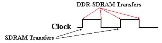
In
“plain” SDRAM, the transfers all take place on the rising edge of the memory
bus clock. In DDR
SDRAM (Double Data Rate Synchronous DRAM), the transfers
take place on both the rising and falling
clock edges.
More on
SDRAM
“Plain”
SDRAM makes a transfer every cycle of the memory bus.
For a 100 MHz memory bus, we would
have 100 million transfers per second.
DDR–SDRAM
is Double Data Rate SDRAM
DDR–SDRAM
makes two transfers for every cycle of the memory bus,
one on the rising edge of the
clock cycle
one on the falling edge of the
clock cycle.
For
a 100 MHz memory bus, DDR–SDRAM would have 200 million transfers per second.
To
this, we add wide memory buses. A
typical value is a 64–bit width.
A
64–bit wide memory bus transfers 64 bits at a time. That is 8 bytes at a time.
Thus
our sample DDR–SDRAM bus would transfer 1,600 million bytes per second.
This
might be called 1.6 GB / second, although it more properly is 1.49 GB / second,
as 1 GB = 1, 073, 741, 824 bytes.
Byte
Addressing vs. Word Addressing
The
addressing capacity of a computer is dictated by the number of bits in the MAR.
Suppose
the MAR (Memory Address Register Contains) N bits.
Then 2N items can be addressed.
In
a byte addressable machine, the maximum memory size is 2N bytes.
If
the machine supports longword addressing, but not byte or word addressing,
the maximum memory size is 2N+2 bytes.
Word
and longword addressable machines might have their
memory sized
quoted in bytes, but they do not access
individual bytes.
Example:
256 KB PDP–11/70 vs. the CDC–6600 with 256 K words (60 bits each).
The
CDC–6600 could have been considered to have 1,920 KB of memory.
However, it was not byte addressable; the
smallest addressable unit was a 60–bit integer.
Almost
every modern computer is byte addressable to allow direct access to the
individual bytes of a character string.
A modern computer that is
byte addressable can still issue both word and longword
instructions. These just reference data two bytes at a time
and four bytes at a time.
Word
Addressing in a Byte Addressable Machine
Each
8–bit byte has a distinct address.
A
16-bit word at address Z contains bytes at addresses Z and Z + 1.
A
32-bit word at address Z contains bytes at addresses
Z, Z + 1, Z + 2, and Z + 3.
Note
that computer architecture refers to addresses, rather than variables.
In
a high–level programming language we use the term “variable” to indicate
the contents of a specific memory address.
Consider
the statement Y = X
Go to the memory address associated with
variable X
Get the contents
Copy the contents into the address
associated with variable Y.
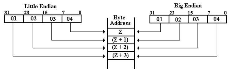
Big–Endian
vs. Little–Endian Addressing

Address Big-Endian Little-Endian
Z 01 04
Z + 1 02 03
Z + 2 03 02
Z + 3 04 01
Example:
“Core Dump” at Address 0x200
Note: Powers of 256 are 2560 = 1, 2561
= 256,
2562
= 65536, 2563 = 16,777,216
Suppose
one has the following memory map as a result of a core dump.
The memory is byte addressable.
|
Address |
0x200 |
0x201 |
0x202 |
0x203 |
|
Contents |
02 |
04 |
06 |
08 |
What is the value of the
32–bit long integer stored at address 0x200?
This is stored in the
four bytes at addresses 0x200, 0x201, 0x202, and 0x203.
Big
Endian: The
number is 0x02040608. Its decimal value
is
2·2563 + 4·2562 + 6·2561 + 8·1 = 33,818,120
Little
Endian: The number is 0x08060402. Its decimal value is
8·2563 + 6·2562 + 4·2561 + 2·1 = 134,611,970.
NOTE: Read the bytes backwards, not the hexadecimal
digits.
Example 2:
“Core Dump” at Address 0x200
Note: Powers of 256 are 2560 = 1, 2561
= 256,
2562
= 65536, 2563 = 16,777,216
Suppose
one has the following memory map as a result of a core dump.
The memory is byte addressable.
|
Address |
0x200 |
0x201 |
0x202 |
0x203 |
|
Contents |
02 |
04 |
06 |
08 |
What is the value of the
16–bit integer stored at address 0x200?
This is stored in the
two bytes at addresses 0x200 and 0x201.
Big
Endian The value is 0x0204.
The decimal
value is 2·256 + 4 = 516
Little
Endian: The value is 0x0402.
The decimal
value s 4·256 + 2 = 1,026
Note: The bytes at addresses 0x202 and 0x203 are
not part of this
16–bit integer.