The Memory Component
The memory stores the instructions
and data for an executing program.
Memory is characterized by the
smallest addressable unit:
Byte
addressable the smallest unit is
an 8–bit byte.
Word
addressable the smallest unit is a
word, usually 16 or 32 bits in length.
Most modern computers are byte
addressable, facilitating access to character data.
Logically, computer memory should be
considered as an array.
The index into this array is called the address
or “memory address”.
A logical view of such a byte
addressable memory might be written in code as:
Const MemSize =
byte Memory[MemSize] // Indexed 0 … (MemSize
– 1)
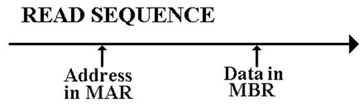
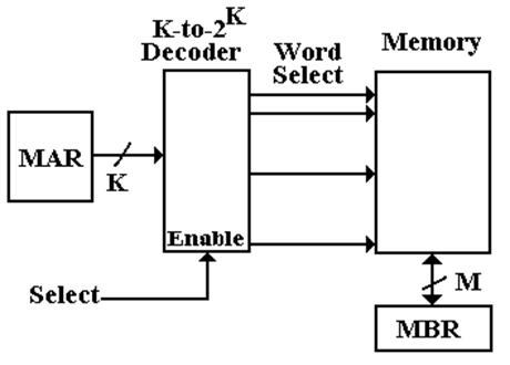
The CPU has two registers dedicated
to handling memory.
The
MAR (Memory Address Register) holds the
address being accessed.
The MBR (Memory Buffer Register) holds the data being written to the
memory
or being read from the memory. This is
sometimes
called the
Memory Data Register.
Requirements
for a Memory Device
1. Random access by
address, similar to use of an array.
Byte addressable
memory can be considered as an
array of bytes.
byte memory [N] // Address ranges from 0 to (N –
1)
2. Binary memory
devices require two reliable stable states.
3. The transitions
between the two stable states must occur quickly.
4. The transitions
between the two stable states must not occur
spontaneously, but only in response
to the proper control signals.
5. Each memory
device must be physically small, so that a large number
may be placed on a single memory
chip.
6. Each memory
device must be relatively inexpensive to fabricate.
Varieties of Random Access Memory
There are two types of RAM
1. RAM read/write
memory
2. ROM read–only
memory.
The double use of the term “RAM” is just accepted. Would you say “RWM”?
Types of ROM
1. “Plain ROM” the
contents of the memory are set at manufacture
and
cannot be changed without destroying the chip.
2. PROM the
contents of the chip are set by a special device
called
a “PROM Programmer”. Once programmed
the
contents are fixed.
3. EPROM same
as a PROM, but that the contents can be erased
and
reprogrammed by the PROM Programmer.
Memory Control Signals
Read / Write Memory must do three actions:
READ copy contents of an addressed word
into the MBR
WRITE copy contents of the MBR into an
addressed word
NOTHING the memory is expected to retain the contents
written into
it until those
contents have been rewritten.
One set of control signals Select# –
the memory unit is selected.
R/W# if 0 the CPU writes to
memory, if 1 the CPU reads from memory.
|
Select# |
R/W# |
Action |
|
0 |
0 |
CPU writes data to the memory. |
|
0 |
1 |
CPU reads data from the memory. |
|
1 |
0 |
Memory contents are not changed. |
|
1 |
1 |
Memory contents are not changed. |
A ROM has
only one control signal: Select.
If Select = 1 for a ROM, the CPU reads data from the
addressed memory slot.
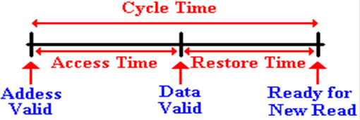
Memory Timings
Memory
Access Time
Defined in terms of reading from memory. It is the time between the address
becoming stable in the MAR and the data becoming available in the MBR.
Memory
Cycle Time
Less used, this is defined as the minimum time between two
independent
memory accesses.
The Memory Bus
The memory bus is a dedicated point–to–point bus between the
CPU and
computer memory. The bus has the
following lines.
1. Address
lines used to select the memory chip
containing the addressed
memory word and to address that
word within the memory.
These
are used to generate the signal Select#,
sent to each memory chip.
2. Data
lines used to transfer data between
the CPU and memory.
3. Bus
Clock is present on a
synchronous bus to coordinate transfers.
4. Control
lines such as the R/W# control
signal mentioned above.
Some
control lines, called strobe lines,
assert the validity of data on
associated lines.
When
RAS (Row Address Strobe) is asserted, the row address on
the
memory address line is certified
to be a valid address.
A Synchronous
Bus Timing Diagram
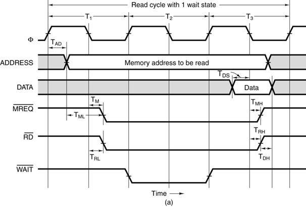
This is a bus read. The sequence: the address becomes valid, RD#
is asserted,
and later the data become valid.
An Asynchronous Bus Timing Diagram
Here,
the importance is the interplay of the Master
Synchronization (MSYN#)
and Slave Synchronization (SSYN#)
signals.
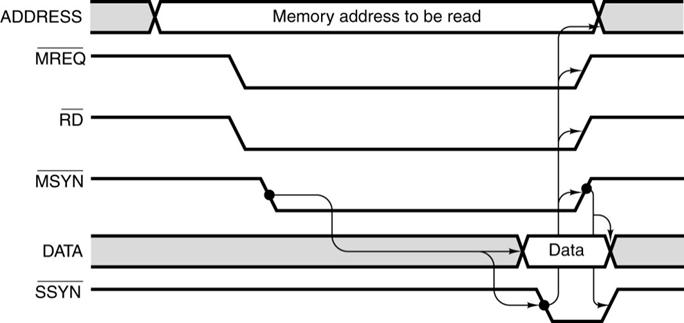
The
sequence: 1. The address becomes valid; MREQ#
and RD# are asserted low.
2. MSYN#
is asserted low, causing the memory to react.
3. Data become valid and SSYN# is asserted low.
4. When SSYN#
goes high, the data are no longer valid.
Sequential Circuits
Sequential
circuits are those with memory, also called “feedback”. In this, they differ
from combinational circuits, which have no memory.
The stable output of a combinational circuit does not depend
on the order in which its
inputs are changed. The stable output of a sequential circuit
usually does depend
on the order in which the inputs
are changed.
Sequential circuits can be used as memory elements; binary
values can be stored in them.
The binary value stored in a circuit element is often called that element’s state.
All sequential circuits depend on a phenomenon called gate delay. This reflects the fact
that the output of any logic gate
(implementing a Boolean function) does not change
immediately when the input
changes, but only some time later.
The gate delay for modern circuits is typically a few nanoseconds.
Synchronous Sequential Circuits
We usually focus on clocked
sequential circuits,
also called synchronous sequential circuits.
As the name “synchronous”
implies, these circuits respond to a system clock,
which is used to synchronize the state changes of the various sequential
circuits.
One textbook claims that “synchronous sequential circuits
use clocks to order events.”
A better claim might be that the clock is used to coordinate events. Events that should
happen at the same time do; events that should happen later do happen later.
The system clock
is a circuit that emits a sequence of regular pulses with a fixed and
reliable pulse rate. If you have an
electronic watch (who doesn’t?), what you have is
a small electronic circuit emitting pulses and a counter circuit to count them.
Clock frequencies are measured in
kilohertz thousands of ticks per second
megahertz millions of ticks per second
gigahertz billions of ticks per second.
One can design asynchronous sequential circuits, which are not controlled by a
system clock.
They present significant design challenges related to timing issues.
Views of the System Clock
There are a number of ways to view the system clock. In general, the view depends on the
detail that we need in discussing the problem.
The logical view is shown in the next figure,
which illustrates some of the terms commonly used for a clock.
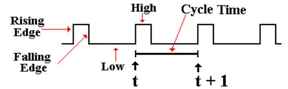
The clock is typical of a periodic function. There is a period t
for which
f(t) = f(t + t)
This clock is asymmetric. It is often the case that the clock is symmetric, where the
time spent at the high level is the same as that at the low level. Your instructor often
draws the clock as asymmetric, just to show that such a design is allowed.
NOTATION: We always call the present clock tick “t” and the next one “t
+ 1”,
even if it occurs only two nanoseconds later.
Views of the System Clock
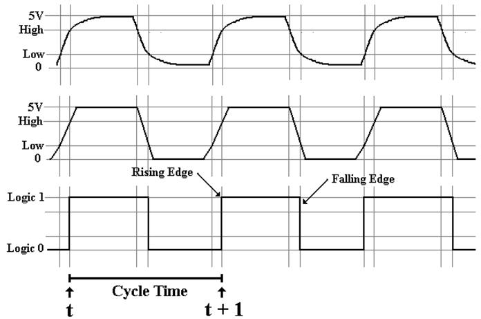
The top view is the “real physical
view”. It is seldom used.
The middle view reflects the fact that voltage levels do not change
instantaneously.
We use this view when considering
system busses.
Clock Period and Frequency
If the clock period is denoted by t,
then the frequency (by definition)
is f = 1 / t.
For example, if t =
2.0 nanoseconds, also written as t =
2.0·10–9 seconds, then
f = 1 / (2.0·10–9 seconds) = 0.50·109 seconds–1
or 500 megahertz.
If f = 2.5
Gigahertz, also written as 2.5·109 seconds–1, then
t = 1.0 / (2.5·109 seconds–1)
= 0.4·10–9 seconds = 0.4 nanosecond.
Memory
bus clock frequencies are in the range 125 to 1333 MHz (1.33 GHz).
CPU
clock frequencies generally are in the 2.0 to 6.0 GHz range, with
2.0 to 3.5 GHz being far the most common.
The
IBM z196 Enterprise Server contains 96 processors, each running at
5.2 GHz. Each processor is water cooled.
Latches
and Flip–Flops: First Definition
We consider a latch or a flip–flop as a device that stores a
single binary value.
Flip–flops and clocked latches are devices that accept input
at fixed times dictated
by the system clock. For this reason
they are called “synchronous sequential
circuits”.
Denote the present time by the symbol t. Denote the clock
period by t.
Rather than directly discussing the clock period, we merely
say that
the current time is t
after the next clock tick the time
is (t + 1)
The present state of the device is often called Q(t)
The next state of the device is often called Q(t
+ 1)
The sequence: the present state is Q(t), the clock “ticks”, the state is now Q(t + 1)
AGAIN: We call the
next state Q(t + 1), even if the transition from
Q(t) to
Q(t + 1) takes only a few nanoseconds. We are counting the actual
number of clock
ticks, not the amount of time they take.
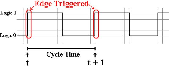
Latches and Flip–Flops: When Triggered
Clocked latches accept input when the system clock is at
logic high.
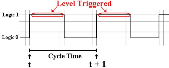
Flip–flops accept input on either the rising edge of the
system clock.
Describing
Flip–Flops
A flip–flop is a “bit
bucket”; it holds a single binary bit.
A flip–flop is characterized by its current state: Q(t).
We want a way to describe the operation of the flip–flops.
How do these devices respond to the input? We use tables to describe the operation.
Characteristic
tables: Given Q(t), the present state of the
flip–flop, and
the
input, what will Q(t + 1), the next state of the
flip–flop, be?
Excitation
tables: Given
Q(t), the present state of the flip–flop, and
Q(t + 1), the desired next state of the flip–flop,
what
input is required to achieve that change.
SR
Flip–Flop
We now adopt a functional view. How does the next state depend on the present
state
and input. A flip–flop is a “bit
holder”.
Here is the diagram for the SR flip–flop.
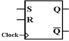
Here
again is the state table for the SR flip–flop.
|
S |
R |
Q(t + 1) |
|
0 |
0 |
Q(T) |
|
0 |
1 |
0 |
|
1 |
0 |
1 |
|
1 |
1 |
ERROR |
Note that
setting both S = 1 and R = 1 causes the flip–flop to enter a logically
inconsistent state, followed by an undeterministic,
almost random, state. For this
reason, we label the output for S = 1 and R = 1 as an error.
JK
Flip–Flop
A JK flip–flop generalizes the SR to allow for both inputs
to be 1.
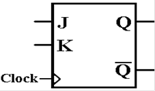
Here
is the characteristic table for a JK flip–flop.
|
J |
K |
Q(t + 1) |
|
0 |
0 |
Q(t) |
|
0 |
1 |
0 |
|
1 |
0 |
1 |
|
1 |
1 |
|
Note that the
flip–flop can generate all four possible functions of a single variable:
the two constants 0 and 1
the variables Q and ![]() .
.
The D Flip–Flop
The D flip–flop specializes either the SR or JK to store a
single bit. It is very useful for
interfacing the CPU to external devices, where the CPU sends a brief pulse to
set the
value in the device and it remains set until the next CPU signal.
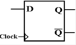
The characteristic table for the D flip–flop is so simple
that it is expressed better as
the equation Q(t + 1) = D. Here is the
table.
|
D |
Q(t
+ 1) |
|
0 |
0 |
|
1 |
1 |
The D
flip–flop plays a large part in computer memory.
Some memory types are just large collections of D
flip–flops.
The other types are not fabricated from flip–flops, but act
as if they were.
The T Flip–Flop
The “toggle” flip–flop allows one to change the value
stored. It is often used in circuits
in which the value of the bit changes between 0 and 1, as in a modulo–4 counter
in which
the low–order bit goes 0, 1, 0, 1, 0, 1, etc.
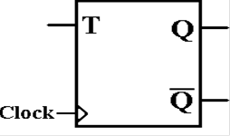
The
characteristic table for the D flip–flop is so simple that it is expressed
better as
the equation Q(t + 1) = Q(t) Å T. Here is the
table.
|
T |
Q(t
+ 1) |
|
0 |
Q(t) |
|
1 |
|
Memory
Mapped Input / Output
Though not a memory issue, we now address the idea of memory
mapped input
and output. In this scheme, we take part
of the address space that would
otherwise be allocated to memory and allocate it to I/O devices.
The PDP–11 is a good example of a memory mapped device. It was a byte
addressable device, meaning that each byte had a unique address.
The old PDP–11/20 supported a 16–bit address space. This supported addresses
in the range 0 through 65,535 or 0 through 0177777 in octal.
Addresses 0 though 61,439 were reserved for physical memory.
In octal these addresses are given by 0 through 167,777.
Addresses 61,440 through 65,535 (octal 170,000 through
177,777) were
reserved for registers associated with Input/Output
devices.
Examples: CR11 Card
Reader 177,160 Control & Status Register
177,162 Data buffer 1
177,164 Data buffer 2
The Linear View of
Memory
Memory may be viewed as a linear array, for example a byte–addressable
memory
byte memory [N] ; // Addresses 0 ..
(N – 1)
This is a perfectly good logical view, it just does not
correspond to reality.
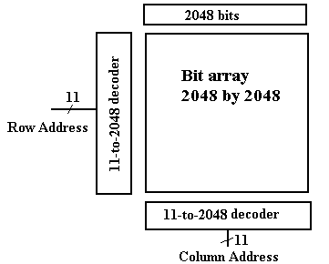
Memory Chip Organization
Consider a 4 Megabit memory chip, in which each bit is
directly addressable.
Recall that 4M = 222 = 211 · 211, and that 211
= 2, 048.
The linear view of memory, on the previous slide, calls for
a 22–to–222 decoder,
also called a 22–to–4,194,304
decoder. This is not feasible.
If we organize the memory as a two–dimensional grid of bits,
then the design
calls for two 11–to–2048
decoders. This is still a stretch.
Managing Pin-Outs
Consider now the two–dimensional memory mentioned
above. What pins are needed?
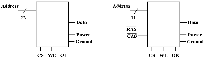
Pin
Count
Address Lines 22 Address
Lines 11
Row/Column 0 Row/Column 2
Power & Ground 2 Power
& Ground 2
Data 1 Data 1
Control 3 Control 3
Total 28 Total 19
Separate
row and column addresses require two cycles to specify the address.
Four–Megabyte Memory
Do we have a single four–megabyte chip or eight four–megabit
memory chips?
One common solution is to have bit–oriented chips. This facilitates the
two–dimensional addressing discussed above.
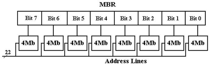
For applications in which data integrity is especially
important, one might add a
ninth chip to hold the parity bit. This
reflects the experience that faults, when
they occur, will be localized in one chip.
Parity provides a mechanism to detect, but not correct,
single bit errors.
Correction of single bit errors requires twelve memory
chips. This scheme will
also detect all two–bit errors.
Memory Interleaving
Suppose a 64MB memory made up of the 4Mb chips discussed
above.
We now ignore parity memory, for convenience and also because it is rarely
needed.
We organize the memory into 4MB banks, each having eight of
the 4Mb chips.
The figure in the slide above shows such a bank.
The memory thus has 16 banks, each of 4MB.
16 = 24 4
bits to select the bank
4M = 222 22 bits address to each chip
Not surprisingly, 64M = 226.
Low–Order Interleaving
|
Bits |
25 – 4 |
3 – 0 |
|
Use |
Address to the chip |
Bank Select |
High–Order
Interleaving (Memory Banking)
|
Bits |
25 – 22 |
21 – 0 |
|
Use |
Bank Select |
Address to the chip |
Most
designs use low order interleaving to reduce effective memory access times.
Faster Memory Chips
We can use the “2 dimensional” array approach, discussed
earlier, to create a faster
memory. This is done by adding a SRAM
(Static RAM) buffer onto the chip.
Consider
the 4Mb (four megabit) chip discussed earlier, now with a 2Kb SRAM buffer.
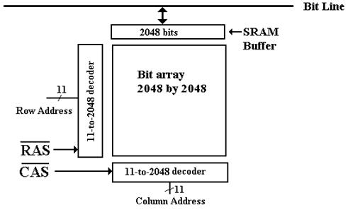
In a modern scenario for reading the
chip, a Row Address is passed to the chip, followed
by a number of column addresses. When
the row address is received, the entire row is
copied into the SRAM buffer. Subsequent
column reads come from that buffer.
Memory Technologies: SRAM and DRAM
One major classification of computer memory is into two
technologies
SRAM Static Random Access Memory
DRAM Dynamic Random Access Memory (and
its variants)
SRAM is called static
because it will keep its contents as long as it is powered.
DRAM is called dynamic
because it tends to lose its contents, even when powered.
Special “refresh circuitry” must be provided.
Compared to DRAM, SRAM is
faster
more expensive
physically larger (fewer memory
bits per square millimeter)
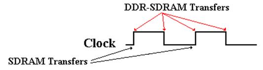
SDRAM is a Synchronous DRAM.
It is DRAM that is designed to work with a Synchronous
Bus, one with a clock signal.
The memory bus clock is driven by the CPU system clock, but
it is always slower.
SDRAM (Synchronous DRAM)
Synchronous Dynamic Random Access Memory
Suppose a 2 GHz system clock. It can easily generate the following memory
bus clock
rates: 1GHz, 500 MHz, 250MHz, 125MHz, etc.
Other rates are also possible.
Consider a 2 GHz CPU with 100 MHz SDRAM.
The CPU clock speed is 2 GHz =
2,000 MHz
The memory bus speed is 100 MHz.
In SDRAM, the
memory transfers take place on a timing dictated by the memory
bus clock rate. This memory bus clock is
always based on the system clock.
In “plain” SDRAM, the transfers all take place on the rising
edge of the memory
bus clock. In DDR SDRAM (Double Data Rate Synchronous DRAM), the transfers
take place on both the rising and falling clock edges.
Speed Up Access by Interleaving Memory
We
have done all we can to make the memory chips faster.
How do we make the memory itself faster with the chips we have?
Suppose
an 8–way low–order interleaved memory.
The chip timings are:
Cycle time: 80
nanoseconds between independent memory reads
Access time 40
nanoseconds to place requested data in the MBR.
Each
chip by itself has the following timing diagram.
This
memory chip can be accessed once every 80 nanoseconds.
The Same Memory with 8–Way Interleaving
Suppose
a set of sequential read operations, beginning at address 1000.
The interleaving is low–order.
Chip
0 has addresses 1000, 1008, 1016, etc.
Chip
1 has addresses 1001, 1009, 1017, etc.
Chip
7 has addresses 1007, 1015, 1023, etc.
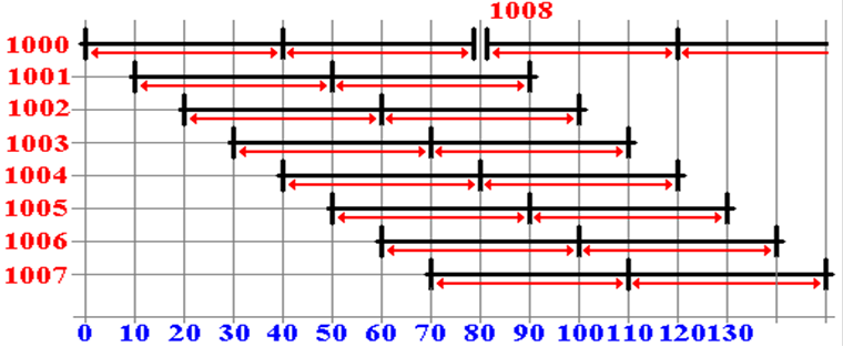
Note
that the accesses can be overlapped, with a net speedup of 8X.
Latency and Bandwidth
Look
again at this figure.

Each
memory bank has a cycle time of 80 nanoseconds.
The
first memory request takes 40 nanoseconds to complete.
The
first time is called latency. This is the time interval between the first
request and its completion.
After
that, there is one result every 10 nanoseconds.
As a bandwidth, this
is 100 million transfers per second.
Fat Data Busses
Here
is another trick to speed up memory transfers.
In
the above example, we assumed that the memory was byte addressable,
having an 8–bit data bus between it and the CPU.
At
one transfer every 10 nanoseconds, this is 100 megabytes per second.
Our
simplistic analysis assumed that these transfers were directly to the CPU.
When
we discuss cache memory, we shall see that the transfers are between
main memory and the L2 (Level 2) cache memory – about 1 MB in size.
Suppose
that the main feature of the L2 cache is an 8–byte cache line.
For
now, this implies that 8 byte transfers between the L2 cache and main
memory are not only easy, but also the most natural unit of transaction.
We
link the L2 cache and main memory with 64 data lines, allowing 8 bytes
to be moved for each memory transfer. We
now have 800 megabytes/sec.
More on SDRAM
“Plain” SDRAM makes a transfer every cycle of the memory
bus.
For a 100 MHz memory bus, we would
have 100 million transfers per second.
DDR–SDRAM is Double Data Rate SDRAM
DDR–SDRAM makes two transfers for every cycle of the memory
bus,
one on the rising edge of the
clock cycle
one on the falling edge of the
clock cycle.
For a 100 MHz memory bus, DDR–SDRAM would have 200 million
transfers per second.
To this, we add wide memory buses. A typical value is a 64–bit width.
A 64–bit wide memory bus transfers 64 bits at a time. That is 8 bytes at a time.
Thus our sample DDR–SDRAM bus would transfer 1,600 million
bytes per second.
This might be called 1.6 GB / second, although it more
properly is 1.49 GB / second,
as 1 GB = 1, 073, 741, 824 bytes.
Evolution of Modern Memory
Here
are some actual cost & performance data for memory.
|
Year |
Cost per MB |
Actual component |
Speed |
Type |
|
|
|
Size (KB) |
Cost |
|
||
|
1957 |
411,041,792.00 |
0.0098 |
392.00 |
10,000 |
transistors |
|
1959 |
67,947,725.00 |
0.0098 |
64.80 |
10,000 |
vacuum tubes |
|
1965 |
2,642,412.00 |
0.0098 |
2.52 |
2,000 |
core |
|
1970 |
734,003.00 |
0.0098 |
0.70 |
770 |
core |
|
1975 |
49,920.00 |
4 |
159.00 |
?? |
static RAM |
|
1981 |
4,479.00 |
64 |
279.95 |
?? |
dynamic RAM |
|
1985 |
300.00 |
2,048 |
599.00 |
?? |
DRAM |
|
1990 |
46.00 |
1,024 |
45.50 |
80 |
SIMM |
|
1996 |
5.25 |
8,192 |
42.00 |
70 |
72 pin SIMM |
|
2001 |
15¢ |
128 MB |
18.89 |
133 MHz |
DIMM |
|
2006 |
7.3¢ |
2,048 MB |
148.99 |
667 MHz |
DIMM DDR2 |
|
2008 |
1.0¢ |
4,096 MB |
39.99 |
800 MHz |
DIMM DDR2 |
|
2010 |
1.22¢ |
8,192 MB |
99.99 |
1333 MHz |
DIMM DDR2 |