The Term “Architecture”
The introduction of the IBM System/360 produced the creation
and
definition of the term “computer
architecture”. According to IBM
[R10]
“The term architecture is used here to
describe the attributes
of a system as seen by the programmer, i.e., the conceptual
structure and functional behavior, as distinct from the
organization of the data flow and controls, the logical design,
and the physical implementation.”
The IBM engineers realized that “logical structure (as seen
by the programmer)
and physical structure (as seen by the engineer) are quite different. Thus, each
may see registers, counters, etc., that to the other are not at all real
entities.”
In more modern terms, we speak of the “Instruction Set Architecture”, or
ISA, of a family of computers. This isolates the logical structure of a CPU
in the family from its physical implementation.
Architecture, Organization, and Implementation
The basic idea behind the IBM System/360 was a family of
computers that
shared the same architecture but had different organization.
For example, each of the computers in the family had 16
general purpose
32–bit registers, numbered 0 through 15.
These were logical constructs.
The organization of the different models called for
registers to be realized
in rather different ways.
Model 30 Dedicated storage locations
in main memory
Models 40 and 50 A dedicated core array, distinct from
main memory.
Models 60, 62, and
70 True data flip–flops, implemented as
transistors.
Strict Program Compatibility
This was the driving goal of the common architecture for the
IBM S/360 family.
IBM issued a precise definition for its goal that all models
in the S/360 family
be “strictly program compatible”; i.e., that they implement the same
architecture. [R10, page 19].
A family of computers is defined to be strictly program
compatible if and
only if a valid program that runs on one model will run on any model.
There are a few restrictions on this definition.
1. The program must be valid. “Invalid programs, i.e., those which
violate the programming manual,
are not constrained to yield
the same results on all models”.
2. The program cannot require more primary memory
storage or types of
I/O devices not available on the
target model.
3. The logic of the program can contain time
dependencies only if they
are explicit; e.g., explicit
testing for event completion.
Instruction Set
Architecture
The
Instruction Set Architecture of a computer defines the view of the machine
as seen by the assembly language programmer.
The
ISA includes the following:
1. The
list of machine language instructions.
2. The
general purpose registers that can be directly accessed
by an assembly language program.
3. The
status flags that are interpreted by conditional instructions
in the machine language.
4. The
standard instructions used to invoke operating system services.
5. The
address modes used and methods to form an effective
address.
6. Indirectly,
the organization of memory (big endian or little endian)
The
ISA can be seen as a contract, specifying the hardware services that
are available to the software. It is the
software–hardware interface.
Comments on the
ISA
Machine Language vs. Assembly Language
The
terms can almost be interchanged, as the concepts are similar.
Consider
an example from the IBM System/370.
Assembly
language: AR 6,8 Add register 8 to register 6
Machine
language: 1A 68 The machine language for the above.
The
term “AR” is the assembly mnemonic for the add
register instruction.
The
term “1A” is the opcode for the add register
instruction.
In binary it is the 8–bit code “0001 1010”.
In
general, each assembly language instruction is translated to
exactly one line of machine language.
Assembly
language is often viewed as a human readable form of
machine language.
It
is for these reasons that we often consider the two languages to be equivalent.
The “Core” Assembly Language
Most
courses teach only a subset of any given assembly language.
This
language, often called the “core assembly language”
suffices to write meaningful programs,
but does not cover the entire range of
extended possibilities.
A
working knowledge of the core assembly language of a given computer
generally leads to a detailed knowledge of its Instruction Set Architecture.
Assembly
languages evolve in time, just as the computers for which they
are written also evolve.
Hardware
features are added to improve CPU performance.
These lead to new assembly language instructions to use those features.
The
standard core assembly languages taught are:
Intel 80386 assembly language, the
basis for the Pentium languages.
IBM System/370 assembly language, the
basis for all IBM mainframes.
What Registers
are Seen?
In
general, the set includes all integer registers and floating–point registers.
On
the IBM System/370, the set would include the following.
The sixteen general–purpose registers
R0 through R15.
The four floating–point registers: F0,
F2, F4, and F6.
For
the Intel Pentium series, the set includes at least the following.
The
four main computational registers (EAX, EBX,
ECX, and EDX), as
well as their subset registers (AX, AH,
AL, BX, BH,
BL, etc.)
The
index registers (EDI and ESI)
and their subsets (DI and SI).
The
32–bit pointer registers (EBP, ESP,
and EIP).
The
16–bit pointer registers (BP, SP,
and IP) and the 16–bit segment
registers (CS, DS,
ES, and SS).
Internal
control registers (MAR, MBR, etc.) are generally not in the ISA.
What is IA–32?
The
term “IA–32” refers to the commonalities
that almost all Intel designs
since the Intel 80386 share.
In
this view, there are roughly three generations of processors in
the main line of Intel products.
IA–16
There
are only three common models in this line:
the Intel 8086 (and 8088), the Intel 80186 (not much used), and Intel 80286.
IA–32
This
class holds all of the 32–bit designs in the Intel main line, beginning with
the Intel 80386 and Intel 80486. All
32–bit Pentium designs are included here.
It
is the upward compatibility design
principle that holds IA–32 together.
IA–64
This
class holds the newer 64–bit Pentium designs.
Status Flags
The
status flags are generally 1–bit values, treated as Boolean, that indicate
the status of program execution and reflect the results of the last
computation.
These
status bits are often grouped together conceptually as a 32–bit PSW
(Program Status Word) or PSR (Program Status Register).
Here
are some values used by the IA–32 designs.
T the
trap bit. This indicates the program is
to be single stepped.
Execution of a program one step
at a time helps to debug.
O Arithmetic
overflow bit. Other designs call this “V”.
S Sign
bit from the ALU. If 1, the result was
negative.
Other designs call this “N”
for negative.
Z Zero
bit from the ALU. If 1, the result was
zero.
C Carry
bit from the ALU. Used in multiple
precision arithmetic.
Invoking
Services of the Operating System
This
class of instructions generates what is called a software interrupt.
On
various designs, these instructions have mnemonics such as
“int” – interrupt, “trap”,
and “svc” – supervisor call.
Some
systems use the name “supervisor” for the operating system.
This
class of instructions is required because of the existence of
privileged instructions that only
the operating system is allowed to execute.
In
the IA–32 designs, the most common of these is the “int 21” series,
which causes a software interrupt with the argument value 21.
The
int 21 series provides input, output, and file
management services.
In
a later chapter, we shall study software interrupts a bit more and answer
a few questions.
1. How
do software interrupts differ from hardware interrupts?
2. How
do software interrupts differ from standard procedure calls?
Data Types:
Basic and Otherwise
The
choice of data types at the ISA level differs slightly from the choice
at the level of a high–level language.
In
Java, one may define a data type and write specific code to handle any
number of operations on that data type.
At
the ISA level, the choice is which data types to support and
how each type is to be supported.
There
are two types of support at the ISA level: hardware and software.
Certain
data types are supported by almost all machines.
Character
Characters
are moved and compared.
Binary Integer
There
are often several integer formats.
Each must be moved, compared, and used in standard arithmetic operations.
More (Basic)
Data Types
Floating Point
Most
computers now support floating point with a special hardware unit.
Almost
all support the two common formats in the IEEE–754 standard.
F IEEE
Single Precision 7 significant digits
in decimal form.
D IEEE
Double Precision 16 significant digits in
decimal form.
NOTE: The IA–32 design uses an internal 80–bit
representation
in order not to lose
precision when accumulating results.
NOTE: Many designs do not directly support single
precision, but
first convert the values to
double precision, do the math,
and then convert back to
single precision.
Packed Decimal
All
IA–32 designs and all IBM Mainframes provide hardware support
for this format, widely used in commercial transactions.
Data Types
Generally Supported in Software
Here
are a few data types that could be supported in hardware.
These
types do not get enough use to warrant the extra expense of creating
special hardware to handle them on most machines.
Bignums
This
is the LISP name for integers (and other numbers) with arbitrarily large
numbers of digits. This would be used to
compute the value of the math
constant π to 100,000 decimal places.
I have seen that done.
Complex Numbers
This
is a set of numbers that has wide applicability in engineering studies.
Complex numbers are often written as x + i·y, were the
symbol i represents
the square root of –1, which is not a real number.
Complex
numbers are normally supported in software as pairs of real numbers,
such as (x, y) for x + i·y. The math rules are implemented in software.
Addition: (x1, y1)
+ (x2,
y2)
= (x1 + x2 , y1 + y2)
Multiplication: (x1, y1)
· (x2,
y2)
= (x1
· x2–
y1
· y2, x1
· y2
+ y1
· x2)
Why Multiple
Precisions?
A
standard ALU (Arithmetic Logic Unit) will support multiple precisions
for representing integers and real numbers.
In
addition, most designs support both signed and unsigned integers.
Why
not support only the most general of each type.
Integers: 64–bit
two’s complement, and
Floats: 64–bit
IEEE–754 double precision?
There
are two standard reasons, each of which is less important for
computation on most standard IA–32 and IA–64 machines.
1. More
effective use of memory.
Why use 8 bytes (64 bits) if 2
bytes (16 bits) will do?
2. Computational
efficiency: arithmetic operations on the larger
data types take somewhat longer
to execute.
Example:
Evolution of Graphics Standards
An
examination of the MS–Windows utility program Paint will show the
evolution of standards for representing color graphics data.
The
original VGA mode allowed for display of only 256 distinct colors
in a 640–by–480 array of pixels. Eight
bits were used to encode each pixel.
Twenty–four
bit color, with eight bits to represent each of the Red, Green,
and Blue values, was introduced along with the hardware to support it.
Recent
graphics standards seem to use IEEE–754 Single Precision floating
point values (presumably one per color) to represent pixel color values.
The
company NVIDIA, a producer of graphics coprocessor cards, included
support for IEEE–754 single precision on its early graphics cards because
it was required to support the standard.
This
gave rise to the CUDA (Compute Unified Device Architecture), in
which NVIDIA graphics cards were used as small supercomputers.
This
gave rise to support for IEEE–754 double precision, a bit slower.
Fixed–Length and
Variable–Length Instructions
In
a modern stored program computer, all instructions share a basic format.
There
are two parts:
1. The
op–code, indicating what instruction is to be executed, and
2. The
rest of the instruction, perhaps containing arguments.
In
a fixed–length instruction design,
all machine language instructions
have the same length. For many designs,
this length is 32 bits or four bytes.
In
a variable–length instruction
design, the length of the instruction varies.
In these, bit patterns in the first bytes of the machine language instruction
are interpreted to determine the length of the instruction.
The
advantages of a fixed–length instruction are seen in the CU (Control Unit)
of the CPU (Central Processing Unit), which can be simpler and faster.
The
disadvantage of such a design is that it makes less efficient use of memory.
Such designs are said to have poor “code
density” in that a smaller percentage
of the memory set aside for code actually contains useful information.
One Example of
Poor Code Density
The
Boz–7 is a didactic design by your instructor.
Each
instruction occupies 32 bits, the first five of which are the op–code.
|
Bit |
31 |
30 |
29 |
28 |
27 |
26 |
25 – 0 |
|
Use |
5–bit opcode |
Address
Modifier |
Use depends on
the opcode |
||||
Now consider the
HALT instruction (op–code = 00000) that stops the computer.
|
Bit |
31 |
30 |
29 |
28 |
27 |
26 |
25 – 0 |
|
Use |
00000 |
Not used |
Not used |
||||
Only 5 of the 32
bits in this instruction mean anything.
Code density = 15.6%.
In
a variable–length–instruction design machine, this probably would
be packaged as an 8–bit instruction.
|
Bit |
7 |
6 |
5 |
4 |
3 |
2 |
1 |
0 |
|
Use |
00000 |
Not used |
||||||
The code density
here is 62.5%
The MIPS
The
MIPS (Microprocessor without Interlocked
Pipeline Stages) is a
commercial design with a fixed length instruction, sized at 32 bits.
The MIPS core
instruction set has about 60 instructions in three basic formats.
The most
significant six bits representing the opcode.
This allows at most 26 = 64 different instructions.
Many arithmetic
operations have the same opcode, with a function selector,
funct,
selecting the function.
For
addition, opcode = 0 and funct = 32.
For subtraction, opcode = 0 and funct = 34. This
makes better use of memory.
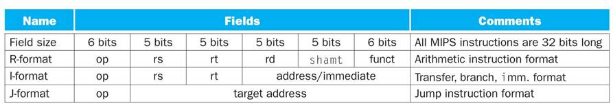
Comments on the
MIPS Design
Note
the three fields (rs, rt,
rd), each designating a general purpose
register.
Each
is a 5–bit field, suggesting a design with 25 = 32 general purpose
registers.
The
shift amount field (shamt) also is a
5–bit field, encoding an unsigned
integer between 0 and 31 inclusive. This
suggests 32–bit registers.
The
address/immediate field in the
I–Format instruction occupies 16 bits.
As an unsigned integer, this would limit memory references to 64KB.
We
infer that this value is a signed address offset; with values in the range
–32768 to +32767. The target address
might be of the form (EIP) + Offset.
The
J–Format target address is a 26 bit value.
This has the potential to
generate direct memory addresses.
All
instructions are four bytes in length and must be aligned on an address that
is a multiple of 4. The last two bits in
the address must be “00”.
This
trick expands the address to 28 bits. 228
bytes = 256 megabytes.
The IBM
System/360 and System/370
The
design for this architecture was formalized in the early 1960’s,
when computer memory was very expensive and somewhat unreliable.
This
design calls for five common instruction formats.
Format Length Use
Name in
bytes
RR 2 Register
to register transfers and arithmetic.
RS 4 Register
to storage and register from storage
RX 4 Register
to indexed storage
and
register from indexed storage
SI 4 Storage
immediate
SS 6 Storage–to–Storage. These have two variants.
The
average instruction length is probably 4 bytes, which represents a
saving of 33% over a fixed–length instruction set, each with 6 bytes.
One Classification of Architectures
How do we handle the operands? Consider a simple addition, specifically
C = A + B
Stack
architecture
In this all operands are
found on a stack. These have good code
density (make good use of memory), but have problems with access.
Typical instructions would include:
Push X // Push the value at address
X onto the top of stack
Pop Y // Pop the top of stack into address Y
Add //
Pop the top two values, add them, & push the result
Program implementation of C = A + B
Push A
Push B
Add
Pop C
Single Accumulator Architectures
There is a single register used to accumulate results of
arithmetic operations.
Consider the high–level language statement C = A + B
Load A //
Load the AC from address A
Add B // Add
the value at address B
Store C // Store the
result into address C
In each of these instructions, the accumulator is implicitly
one of the operands
and need not be specified in the
instruction. This saves space.
Extension
of this for multiplication
If we multiply two 16–bit signed integers, we can get a 32–bit result.
Consider squaring 24576 (214 + 213) or 0110 0000 0000
0000 is 16–bit binary.
The result is 603, 979, 776 or 0010 0100 0000 0000 0000 0000
0000 0000.
We need two 16–bit registers to hold the result. The PDP–9 had the MQ and AC.
The results of this multiplication would be
MQ 0010 0100 0000 0000 //
High 16 bits
AC 0000 0000 0000 0000 //
Low 16 bits
General Purpose Register Architectures
These have a number of general purpose registers, normally
identified by number.
The number of registers is often a power of 2: 8, 16, or 32
being common.
(The Intel architecture with its four general purpose
registers is different. These are
called EAX, EBX, ECX, and EDX – a
lot of history here)
The names of the registers often follow an assembly language
notation designed to
differentiate register names from
variable names. An architecture with
eight general
purpose registers might name them:
%R0, %R1, …., %R7.
The prefix “%” here indicates to the assembler that we are
referring to a register, not to
a variable that has a name such as
R0. The latter name would be poor coding
practice.
Designers might choose to have register %R0 identically set
to 0. Having this constant
register considerably simplifies a
number of circuits in the CPU control unit.
General Purpose Registers with Load–Store
A Load–Store
architecture is one with a number of general purpose registers in
which the only memory references
are:
1) Loading a register from memory
2) Storing a register to memory
The realization of our programming statement C = A + B might
be something like
Load
%R1, A // Load memory location A contents into register 1
Load
%R2, B // Load register 2 from memory location B
Add
%R3, %R1, %R2 // Add contents of
registers %R1 and %R2
//
Place results into register %R3
Store
%R3, C // Store register 3 into memory location C
The
load–store approach was pioneered by the RISC
(Reduced Instruction Set
Computing) movement, to be discussed
later in this lecture.
General Purpose Registers: Register–Memory
In a load–store architecture, the operands for any
arithmetic operation must all be in CPU
registers. The Register–Memory
design relaxes this requirement to requiring only one
of the operands to be in a register.
We might have two types of addition instructions
Add register
to register
Add memory to register
The realization of the above simple program statement, C = A
+ B, might be
Load %R4, A //
Get M[A] into register 4
Add %R4, B // Add M[B]
to register 4
Store %R4, C // Place
results into memory location C
General Purpose Registers: Memory–Memory
In this, there are no restrictions on the location of
operands.
Our instruction C = A + B might be encoded simply as
Add C, A, B
The VAX series supported this mode.
The VAX had at least three different addition instructions
for each data length
Add register to register
Add memory to register
Add memory to memory
There were these three for each of the following data types:
8–bit bytes, 16–bit integers, and
32–bit long integers
32–bit floating point numbers and
64–bit floating point numbers.
Here we see at least 15 different instructions that perform
addition. This is complex.
Reduced
Instruction Set Computers
The acronym RISC stands for “Reduced Instruction Set Computer”.
RISC represents a design philosophy for the ISA (Instruction
Set Architecture) and
the CPU microarchitecture that implements that ISA.
RISC is not a set of rules; there is no “pure RISC” design.
The first designed called “RISC” date to the early
1980’s. The movement began with
two experimental designs
The IBM 801 developed
by IBM in 1980
The RISC I developed by UC Berkeley in 1981.
We should
note that the original RISC machine was probably the CDC–6400 designed
and built by Mr. Seymour Cray, then of the Control Data Corporation.
In designing a CPU that was simple and very fast, Mr. Cray
applied many of the techniques
that would later be called “RISC” without himself using the term.
RISC vs. CISC Considerations
The acronym CISC, standing for “Complex Instruction Set Computer”, is a term applied
by the proponents of RISC to computers that do not follow that design.
Early CPU designs could have followed the RISC philosophy,
the advantages
of which were apparent early. Why then
was the CISC design followed?
Here are two reasons thought to be important:
1. CISC designs make
more efficient use of memory. In
particular, the “code
density” is better, more
instructions per kilobyte.
The cost of
memory was a major design influence until the late 1990’s.
2. CISC designs
close the “semantic gap”; they produce an ISA with
instructions that more closely
resemble those in a higher–level language.
This should provide better support
for the compilers.
The VAX–11/780, manufactured in the 1970’s and 1980’s was
definitely CISC,
a fact that lead to its demise. The
complexity of its control unit made it
much too slow.
RISC vs. CISC Considerations
The RISC (Reduced
Instruction Set Computer) movement advocated a simpler design
with fewer options for the instructions.
Simpler instructions could execute faster.
One of the main motivations for the RISC movement is the
fact that computer memory
is no longer a very expensive
commodity. In fact, it is a “commodity”;
that is, a
commercial item that is readily and
cheaply available.
If we have fewer and simpler instructions, we can speed up
the computer’s speed
significantly. True, each instruction might do less, but
they are all faster.
The
Load–Store Design
One of the slowest operations is the access of memory, either to read values
from it or
write values to it. A load–store
design restricts memory access to two instructions
1) Load
a register from memory
2) Store
a register into memory
A moment’s reflection will show that this works only if we
have more than one register,
possibly 8, 16, or 32
registers. More on this when discussing
the options for operands.
NOTE: It is easier to write a good compiler for an
architecture with a lot of registers.
Modern
Design Principles: Basic Assumptions
Some assumptions that drive current design practice include:
1. The fact that most programs are written in
high–level compiled
languages. Provision of a large general purpose register
set
greatly facilitates compiler
design.
2. The fact that current CPU clock cycle times
(0.25 – 0.50 nanoseconds)
are
much faster than memory access times.
Reducing
the number of memory accesses will speed up the program.
3. The fact that a simpler instruction set
implies a smaller control unit,
thus freeing chip area for
more registers and on–chip cache.
4. The fact that execution is more efficient
when a two level cache
system is implemented
on–chip. We have a split L1 cache (with
an I–Cache for instructions
and a D–Cache for data) and a L2 cache.
5. The fact that memory is so cheap that it is
a commodity item.
Modern Design Principles
1. Allow only
fixed–length operands. This may waste
memory, but modern
designs have plenty of it, and it
is cheap.
2. Minimize the
number of instruction formats and make them simpler, so that
the instructions are more easily
and quickly decoded.
3. Provide plenty
of registers and the largest possible on–chip cache memory.
4. Minimize the
number of instructions that reference memory.
Preferred
practice is called “Load/Store” in
which the only operations to reference
primary memory are: register loads from memory
register
stores into memory.
5. Use pipelined
and superscalar approaches that attempt to keep each unit
in the CPU busy all the time. At the very least provide for fetching one
instruction while the previous
instruction is being executed.
6. Push
the complexity onto the compiler. This
is called moving the DSI
(Dynamic–Static interface). Let Compilation (static phase) handle any
any issue that it can, so that
Execution (dynamic phase) is simplified.
What
About Support for High Level Languages?
Experimental studies conducted in 1971 by Donald Knuth and
in 1982 by David Patterson showed that
1) nearly 85% of a programs statements were
simple assignment,
conditional, or procedure calls.
2) None of these required a complicated
instruction set.
The following table summarizes some results from
experimental studies of code
emitted by typical compilers of the 1970’s and 1980’s.
|
Language |
Pascal |
FORTRAN |
Pascal |
C |
SAL |
|
Workload |
Scientific |
Student |
System |
System |
System |
|
Assignment |
74 |
67 |
45 |
38 |
42 |
|
Loop |
4 |
3 |
5 |
3 |
4 |
|
Call |
1 |
3 |
15 |
12 |
12 |
|
If |
20 |
11 |
29 |
43 |
36 |
|
GOTO |
2 |
9 |
-- |
3 |
-- |
|
Other |
|
7 |
6 |
1 |
6 |
Comparison
of RISC and CISC
This table is taken from an IEEE tutorial on RISC
architecture.
|
|
CISC
Type Computers |
RISC
Type |
|||
|
|
IBM 370/168 |
VAX-11/780 |
Intel 8086 |
RISC I |
IBM 801 |
|
Developed |
1973 |
1978 |
1978 |
1981 |
1980 |
|
Instructions |
208 |
303 |
133 |
31 |
120 |
|
Instruction size (bits) |
16 – 48 |
16 – 456 |
8 – 32 |
32 |
32 |
|
Addressing Modes |
4 |
22 |
6 |
3 |
3 |
|
General Registers |
16 |
16 |
4 |
138 |
32 |
|
Control Memory Size |
420 Kb |
480 Kb |
Not given |
0 |
0 |
|
Cache Size |
64 Kb |
64 Kb |
Not given |
0 |
Not given |
Experience on the VAX
by Digital Equipment Corporation (DEC)
The VAX–11/780 is the classic CISC design with
a very complex instruction set.
DEC experimented with two different implementations of the
VAX architecture.
These are the VLSI VAX and the MicroVAX–32.
The VLSI VAX implemented the entire VAX instruction set.
The MicroVAX–32 design was based on the following
observation about the
more complex instructions.
they account for
20% of the instructions in the VAX ISA,
they account for
60% of the microcode, and
they account for
less than 0.2% of the instructions executed.
The MicroVAX implemented these instructions in system
software.
Results of the DEC Experience
The VLSI VAX uses five to ten times the resources of the
MicroVAX.
The VLSI VAX is only about 20% faster than the MicroVAX.
Here is a table from their study.
|
|
VLSI VAX |
MicroVAX 32 |
|
VLSI Chips |
9 |
2 |
|
Microcode |
480K |
64K |
|
Transistors |
1250K |
101K |
Notes: 1. The
MicroVAX used two VLSI chips”
One for the basic
instruction set, and
one for the optional
floating–point processor.
2. Note that two MicroVAX–32 computers, used
together,
might have about 160%
of the performance of the VLSI VAX
at about half the
cost.
The RISC/360
The term is this author’s name for an experiment by David A.
Patterson.
The IBM System/360 comprises a number of computers, all of
which
fall definitely in the CISC category.
Each has a complex instruction set.
Patterson’s experiment focused on the IBM S/360 and S/370 as
targets for a
RISC compiler. One model of interest was
the S/360 model 44.
A compiler created for the RISC computer IBM 801 (an early
RISC design) was
adapted to emit code for the S/370 treated as a load–store RISC machine.
This subset ran programs 50 percent faster than the previous
best optimizing
compiler that used the full S/360 instruction set.
Reference
David A. Patterson, Reduced
Instruction Set Computers, Communications of the
ACM, Volume 28, Number 1, 1985.
Reprinted in IEEE Tutorial Reduced
Instruction Set Computers , edited by William Stallings, The Computer Science
Press, 1986, ISBN 0–8181–0713–0.