Consider
a Boolean function of two Boolean variables X and Y. The only possibilities for
the values of the variables are:
X = 0 and
Y = 0
X = 0 and
Y = 1
X = 1 and
Y = 0
X = 1 and
Y = 1
Similarly,
there are eight possible combinations of the three variables X, Y, and Z,
beginning
with X = 0, Y = 0, Z = 0 and going through X = 1, Y = 1, Z = 1. Here they are.
X = 0, Y = 0, Z = 0 X = 0, Y = 0, Z = 1 X = 0, Y = 1, Z = 0 X = 0, Y = 1, Z = 1
X = 1, Y = 0, Z = 0 X = 1, Y = 0, Z = 1 X = 1, Y = 1, Z = 0 X = 1, Y = 1, Z = 1
As we shall see, we prefer truth tables for functions of not too many
variables.
|
X
|
Y
|
F(X,
Y)
|
|
0
|
0
|
1
|
|
0
|
1
|
0
|
|
1
|
0
|
0
|
|
1
|
1
|
1
|
The
figure at left is a truth table for a two-variable function. Note that
we have four rows in the truth table, corresponding to the four possible
combinations of values for X and Y. Note
also the standard order in
which the values are written: 00, 01, 10, and 11. Other orders can be
used when needed (it is done below), but one must list all combinations.
|
X
|
Y
|
Z
|
F1
|
F2
|
|
0
|
0
|
0
|
0
|
0
|
|
0
|
0
|
1
|
1
|
0
|
|
0
|
1
|
0
|
1
|
0
|
|
0
|
1
|
1
|
0
|
1
|
|
1
|
0
|
0
|
1
|
0
|
|
1
|
0
|
1
|
0
|
1
|
|
1
|
1
|
0
|
0
|
1
|
|
1
|
1
|
1
|
1
|
1
|
For
another example of truth tables, we consider the figure at
the left, which shows two Boolean functions of three Boolean
variables. Truth tables can be used to
define more than one
function at a time, although they become hard to read if either
the number of variables or the number of functions is too large.
Here we use the standard shorthand of F1 for F1(X, Y, Z) and
F2 for F2(X, Y, Z). Also note the
standard ordering of the
rows, beginning with 0 0 0 and ending with 1 1 1. This causes
less confusion than other ordering schemes, which may be used
when there is a good reason for them.
As
an example of a truth table in which non-standard ordering might be useful,
consider the
following table for two variables. As
expected, it has four rows.
|
X
|
Y
|
X · Y
|
X + Y
|
|
0
|
0
|
0
|
0
|
|
1
|
0
|
0
|
1
|
|
0
|
1
|
0
|
1
|
|
1
|
1
|
1
|
1
|
A
truth table in this non-standard ordering would be used to
prove the standard Boolean axioms:
X ·
0 = 0 for all X X
+ 0 = X for all X
X ·
1 = X for all X X + 1 = 1 for
all X
Note
the identity X + 1 = 1. This is the
“strange Boolean axiom”
that
gives rise to many peculiarities in the logic.
Labeling
Rows in Truth Tables
We
now discuss a notation that is commonly used to identify rows in truth
tables. The exact
identity of the rows is given by the values for each of the variables, but we
find it convenient
to label the rows with the integer equivalent of the binary values. We noted above that for N
variables, the truth table has 2N rows. These are conventionally numbered from 0
through
2N – 1 inclusive to give us a handy way to reference the rows. Thus a two variable truth table
would have four rows numbered 0, 1, 2, and 3.
Here is a truth-table with labeled rows.
|
Row
|
A
|
B
|
G(A,
B)
|
|
0
|
0
|
0
|
0
|
|
1
|
0
|
1
|
1
|
|
2
|
1
|
0
|
1
|
|
3
|
1
|
1
|
0
|
We can see that G(A, B)
= A Å B, but
0 = 0·2
+ 0·1 this value has nothing to do with
the
1 = 0·2
+ 1·1 row numberings, which are just the
2 = 1·2
+ 0·1 decimal equivalents of the values
in
3 = 1·2
+ 1·1 the A & B columns as binary.
A three variable
truth table would have eight rows, numbered 0, 1, 2, 3, 4, 5, 6, and 7.
Here is a three variable truth table for a function F(X, Y, Z) with the rows
numbered.
|
Row
Number
|
X
|
Y
|
Z
|
F(X,
Y, Z)
|
|
0
|
0
|
0
|
0
|
1
|
|
1
|
0
|
0
|
1
|
1
|
|
2
|
0
|
1
|
0
|
0
|
|
3
|
0
|
1
|
1
|
1
|
|
4
|
1
|
0
|
0
|
1
|
|
5
|
1
|
0
|
1
|
0
|
|
6
|
1
|
1
|
0
|
1
|
|
7
|
1
|
1
|
1
|
1
|
Note
that the row numbers correspond to the
decimal value of the three bit binary, thus
0 = 0·4
+ 0·2 + 0·1
1 = 0·4
+ 0·2 + 1·1
2 = 0·4
+ 1·2 + 0·1
3 = 0·4
+ 1·2 + 1·1
4 = 1·4
+ 0·2 + 0·1
5 = 1·4
+ 0·2 + 1·1
6 = 1·4
+ 1·2 + 0·1
7 = 1·4
+ 1·2 + 1·1
Truth tables are
purely Boolean tables in which decimal numbers, such as the row numbers
above do not really play a part.
However, we find that the ability to label a row with a
decimal number to be very convenient and so we use this. The row numberings can be quite
important for the standard algebraic forms used in representing Boolean
functions.
Question:
Where to Put the Ones and Zeroes
Every
truth table corresponds to a Boolean expression. For some truth tables, we begin with
a Boolean expression and evaluate that expression in order to find where to
place the 0’s and
1’s. For other tables, we just place a
bunch of 0’s and 1’s and then ask what Boolean
expression we have created. The truth
table just above was devised by selecting an
interesting pattern of 0’s and 1’s. The
author of these notes had no particular pattern in
mind when creating it. Other truth
tables are more deliberately generated.
Let’s
consider the construction of a truth table for the Boolean expression.
F(X,
Y, Z) = 
Let’s
evaluate this function for all eight possible values of X, Y, Z.
X = 0 Y = 0 Z = 0 F(X, Y, Z) = 0·0
+ 0·0 + 0·1·0
= 0 + 0 + 0 = 0
X = 0 Y = 0 Z = 1 F(X, Y, Z) = 0·0
+ 0·1 + 0·1·1
= 0 + 0 + 0 = 0
X = 0 Y = 1 Z = 0 F(X, Y, Z) = 0·1
+ 1·0 + 0·0·0
= 0 + 0 + 0 = 0
X = 0 Y = 1 Z = 1 F(X, Y, Z) = 0·1
+ 1·1 + 0·0·1
= 0 + 1 + 0 = 1
X = 1 Y = 0 Z = 0 F(X, Y, Z) = 1·0
+ 0·0 + 1·1·0
= 0 + 0 + 0 = 0
X = 1 Y = 0 Z = 1 F(X, Y, Z) = 1·0
+ 0·1 + 1·1·1
= 0 + 0 + 1 = 1
X = 1 Y = 1 Z = 0 F(X, Y, Z) = 1·1
+ 1·0 + 1·0·0
= 1 + 0 + 0 = 1
X = 1 Y = 1 Z = 1 F(X, Y, Z) = 1·1
+ 1·1 + 1·0·1
= 1 + 1 + 0 = 1
From
the above, we create the truth table for the function. Here it is.
|
X
|
Y
|
Z
|
F(X, Y, Z)
|
|
0
|
0
|
0
|
0
|
|
0
|
0
|
1
|
0
|
|
0
|
1
|
0
|
0
|
|
0
|
1
|
1
|
1
|
|
1
|
0
|
0
|
0
|
|
1
|
0
|
1
|
1
|
|
1
|
1
|
0
|
1
|
|
1
|
1
|
1
|
1
|
Consider
the truth table given below, with no explanation of the method used to generate
the
values of F1 and F2 for each row.
|
Row
|
X
|
Y
|
Z
|
F1
|
F2
|
|
0
|
0
|
0
|
0
|
0
|
0
|
|
1
|
0
|
0
|
1
|
1
|
0
|
|
2
|
0
|
1
|
0
|
1
|
0
|
|
3
|
0
|
1
|
1
|
0
|
1
|
|
4
|
1
|
0
|
0
|
1
|
0
|
|
5
|
1
|
0
|
1
|
0
|
1
|
|
6
|
1
|
1
|
0
|
0
|
1
|
|
7
|
1
|
1
|
1
|
1
|
1
|
Figure: Our
Sample Functions F1 and F2
Students
occasionally ask how the author knew where to place the 0’s and 1’s in the
above
table. There are two answers to this,
both equally valid. We reiterate the
statement that a
Boolean function is completely specified by its truth table. Thus, one can just make an
arbitrary list of 2N 0’s and 1’s and then decide what function of N
Boolean variables has
been represented. In that view, the
function F2 is that function specified by the sequence
(0, 0, 0, 1, 0, 1, 1, 1) and nothing more.
We can use methods described below to assign it a
functional representation. Note that F2
is 1 if and only if two of X, Y, and Z are 1.
Given
this, we can give a functional description of the function as F2 = X·Y + X·Z + Y·Z.
As
the student might suspect, neither the pattern of 0’s and 1’s for F1 nor that
for F2 were
arbitrarily selected. The real answer is
that the instructor derived the truth table from a set of
known Boolean expressions, one for F1 and one for F2. The student is invited to compute
the value of F2 = X·Y + X·Z + Y·Z for all possible values of X,
Y, and Z; this will verify
the numbers as shown in the truth table.
We
have noted that a truth table of two variables has four rows (numbered 0, 1, 2,
and 3)
and that a truth table of three variables has eight rows (numbered 0 through
7). We now
prove that a truth table of N variables has 2N rows, numbered 0
through 2N – 1. Here is an
inductive proof, beginning with the case of one variable.
1. Base
case: a function of one variable X requires 2 rows,
one row for X = 0 and one row
for X = 1.
2. If
a function of N Boolean variables X1, X2, …., XN
requires 2N rows, then
the function of (N + 1)
variables X1, X2, …., XN, XN+1
would require
2N rows for X1,
X2, …., XN when XN+1 = 0
2N rows for X1,
X2, …., XN when XN+1 = 1
3. 2N
+2N = 2N+1, so the function of (N + 1) variables required
2N+1 rows.
While
we are at it, we show that the number of Boolean functions of N Boolean
variables is
2R where R = 2N, thus the number is  . The argument is
quite simple. We have shown
. The argument is
quite simple. We have shown
that the number of rows in a truth table is given by R = 2N. The value in the first row could
be a 0 or 1; thus two choices. Each of
the R = 2N rows could have two choices, thus the total
number of functions is 2R where R = 2N.
For
N = 1, R = 2, and 22 = 4. A
truth table for the function F(X) would have two rows, one
for X = 0 and one for X = 1. There are
four functions of a single Boolean variable.
F1(X) = 0, F2(X)
= 1, F3(X) = X, and F4(X) =  .
.
It
might be interesting to give a table of the number of rows in a truth table and
number of
possible Boolean functions for N variables.
The number of rows grows quickly, but the
number of functions grows at an astonishing rate.
|
N
|
R
= 2N
|
2R
|
|
1
|
2
|
4
|
|
2
|
4
|
16
|
|
3
|
8
|
256
|
|
4
|
16
|
65
536
|
|
5
|
32
|
4
294 967 296
|
|
6
|
64
|
264
» 1.845·1019
|
Note
on computation: log 2 = 0.30103, so 264
= (100.30103)64 = 1019.266 .
log 1.845 = 0.266,
so 100.266 » 1.845 and 1019.266
» 1.845·1019
The
number of Boolean functions of N Boolean variables is somewhat of
interest. More to
interest in this course is the number of rows in any possible truth–table
representation of a
function of N Boolean variables. For N =
2, 3, and 4, we have 2N = 4, 8, and 16 respectively,
so that truth tables for 2, 3, and 4 variables are manageable. Truth tables for five variables
are a bit unwieldy and truth tables for more than five variables are almost
useless.
Evaluation of Boolean Expressions
Here is another topic that this
instructor normally forgets to mention, as it is so natural to
one who has been in the “business” for many years. The question to be addressed now is:
“What are the rules for evaluating Boolean expressions?”
Operator Precedence
The main question to be addressed is
the relative precedence of the basic Boolean operators:
AND, OR, and NOT. These rules are based
on the algebraic model, which does not use the
XOR function; its precedence is not defined.
The relative precedence in any programming
language is specified by that language.
The relative precedence of the
operators is:
1) NOT do this first
2) AND
3) OR do this last
Consider the Boolean expression A·B + C·D,
often written as AB + CD. Without the
precedence rules, there are two valid interpretations: either (A·B) + (C·D)
or A·(B + C)·D.
The precedence rules for the operators indicate that the first is the correct
interpretation; in
this Boolean algebra follows standard algebra as taught in high-school. Consider now the
expression  ; according to our rules, this is read as
 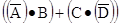 .
.
Note that parentheses and explicit
extension of the NOT over–bar can override the precedence
rules, so that A·(B
+ C)·D is read as the logical AND of
three terms: A, (B + C), and D.
Note also that the two expressions  and
and  are
different. The first expression, better
are
different. The first expression, better
written as  , refers to the logical NOT of the logical AND of A
and B; in a language
, refers to the logical NOT of the logical AND of A
and B; in a language
such as LISP it would be written as NOT (AND A B). The second expression, due to the
precedence rules, refers to the logical AND of the logical NOT of A and the
logical NOT
of B; in LISP this might be written as AND( (NOT A) (NOT B) ).
Evaluation of Boolean expressions
implies giving values to the variables and following the
precedence rules in applying the logical operators. Let A = 1, B = 0, C = 1, and D = 1.
A·B + C·D
= 1·0 + 1·1 = 0 + 1 = 1
A·(B + C)·D
= 1·(0 + 1)·1 = 1 ·
1 · 1 = 1
=  = 0 · 0 + 1 ·
0 = 0 + 0 = 0
= 0 · 0 + 1 ·
0 = 0 + 0 = 0
=  =
=  = 1
= 1
=  = 0 · 1 = 0
Also A·(B + C·D)
= 1·(0 + 1·1) = 1 ·
(0 + 1) = 1 · 1 = 1
(A·B + C)·D
= (1·0 + 1)·1 = (0 + 1) ·
1 = 1
In Boolean algebra we have the distributive postulate A·(B + C) = A·B
+ A·C, which looks
familiar. We also have the rather
strange postulate A + B·C
= (A + B)·(A + C) must also be
true. We prove the second statement
using a method unique to Boolean algebra.
This method
depends on the fact that there are only two possible values for A: A = 0 and A
= 1. We consider
both cases using a proof technique much favored by this instructor: consider
both possibilities for
one variable. Again, the statement is
that the following is a Boolean identity
A + B·C = (A + B)·(A + C).
If A = 1, the statement becomes 1 + B·C = (1 + B)·(1
+ C), or 1 = 1·1,
obviously true.
If A = 0, the statement becomes 0 + B·C = (0 + B)·(0
+ C), or B·C = B·C.
Just for fun, we offer a truth–table proof of the second
distributive postulate.
|
A
|
B
|
C
|
B·C
|
A + B·C
|
|
(A
+ B)
|
(A
+ C)
|
(A + B)·(A + C)
|
|
0
|
0
|
0
|
0
|
0
|
|
0
|
0
|
0
|
|
0
|
0
|
1
|
0
|
0
|
|
0
|
1
|
0
|
|
0
|
1
|
0
|
0
|
0
|
|
1
|
0
|
0
|
|
0
|
1
|
1
|
1
|
1
|
|
1
|
1
|
1
|
|
1
|
0
|
0
|
0
|
1
|
|
1
|
1
|
1
|
|
1
|
0
|
1
|
0
|
1
|
|
1
|
1
|
1
|
|
1
|
1
|
0
|
0
|
1
|
|
1
|
1
|
1
|
|
1
|
1
|
1
|
1
|
1
|
|
1
|
1
|
1
|
Figure: A + B·C = (A +
B)·(A + C)
Note that
to complete the proof, one must construct the truth table, showing columns for
each of the two functions A + B·C
and (A + B)·(A + C), then note that the contents
of the
two columns are identical for each row.
Implementation of Boolean Logic by
Circuitry
We
now turn to a study of the digital gates used to implement the standard Boolean
functions.
The Boolean values are represented by specific voltages in the electronic
circuitry. As a
result of experience, it has been found desirable only to have two voltage
levels, called High
and Low or H and L. This leads to two
types of logic
Negative Logic High = 0 Low = 1
Positive Logic High = 1 Low = 0
This
course will focus on Positive Logic and ignore Negative Logic. As a matter of fact, we
shall only occasionally concern ourselves with voltage levels. There are several varieties of
positive logic, depending on the voltage at which the chip is run. The logic low is always
specified as 0 volts, but the logic high might be 5 volts, 3.5 volts, 1.8
volts, or whatever the
voltage to the CPU chip is set at. This
text will follow the TTL standard voltages established
by Texas Instruments, in which the logic high level is specified to be 5.0
volts. In reality,
voltage ranges are specified. The range
for output is stricter than that for input to allow for
voltage degradation during transmission.
Output of Logic
Gate Input to Logic Gate
Logic High 2.4
– 5.0 volts 2.0
– 5.0 volts
Logic
Low 0.0 – 0.4 volts 0.0 – 0.8 volts
Basic Gates for
Boolean Functions
We
now discuss a number of basic logic gates used to implement Boolean
functions. The
gates of interest at this point are AND, OR, NOT, NAND (NOT AND), NOR (NOT OR)
and
XOR (Exclusive OR). The Exclusive OR
gate is the same as the OR gate except that the
output is 0 (False) when both inputs are 1 (True). The symbol for XOR is Å.
The
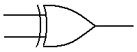
first gate to be discussed is the OR gate.
The truth table for a two-input OR gate is
shown below. In general, if any input to
an OR gate is 1, the output is 1.
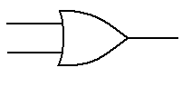 A B A + B
0 0 0
0 1 1
1 0 1
1 1 1
The
next gate to be discussed is the AND gate.
The truth table for a two-input AND gate is
shown now. In general, if any input to
an AND gate is 0, the output is 0.
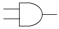 A B A ·
B
A B A ·
B
0 0 0
0 1 0
1 0 0
1 1 1
The
third of the four basic gates is the single input NOT gate. Note that there are two ways
of denoting the NOT function. NOT(A) is
denoted as either A’ or  . We use as often as
possible to represent NOT(A), but may become lazy and use the other notation.
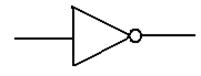
A
0 1
1 0
The
last of the gates to be discussed at this first stage is not strictly a basic
gate. We include
it at this level because it is extremely convenient. This is the two-input Exclusive OR (XOR)
gate, the function of which is shown in the following truth table.
 A B A
Å B
A B A
Å B
0 0 0
0 1 1
1 0 1
1 1 0
We
note immediately an interesting and very useful connection between the XOR
function
and the NOT function. For any A, A Å 0 = A, and A Å 1 =.
The proof is by
truth table.
A B A Å
B Result
0 0 0 A
1 0 1 A This result is extremely useful
when designing
0 1 1 a ripple
carry adder/subtractor.
1 1 0
The
basic logic gates are defined in terms of the binary Boolean functions. Thus, the basic
logic gates are two-input AND gates, two-input OR gates, NOT gates, two-input
NAND
gates, two-input NOR gates, and two-input XOR gates.
It
is common to find three-input and four-input varieties of AND, OR, NAND, and
NOR
gates. The XOR gate is essentially a
two-input gate; three input XOR gates may exist but
they are hard to understand.
Consider
a four input AND gate. The output
function is described as an easy generalization
of the two input AND gate; the output is 1 (True) if and only if all of the
inputs are 1,
otherwise the output is 0. One can
synthesize a four-input AND gate from three two-input
AND gates or easily convert a four-input AND gate into a two-input AND
gate. The student
should realize that each figure below represents only one of several good
implementations.
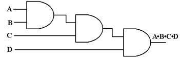
Figure: Three
2-Input AND Gates Make a 4-Input AND Gate
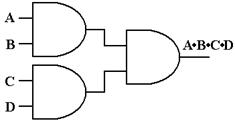
Figure: Another
Way to Configure Three 2-Input AND Gates as a 4-Input AND Gate
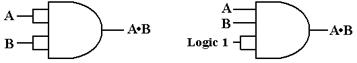
Figure: Two Ways to
Configure a 4-Input AND Gate as a 2-Input AND Gate
Here
is the general rule for N-Input AND gates and N-Input OR gates.
AND Output
is 0 if any input is 0. Output is 1 only
if all inputs are 1.
OR Output
is 1 if any input is 1. Output is 0 only
if all inputs are 0.
XOR For
N > 2, N-input XOR gates are not useful and will be avoided.
NOT By
definition, the NOT gate has only one input.
“Derived Gates”
We now show 2 gates that may be
considered as derived from the above: NAND and NOR.
 The NOR gate is the
same as an OR gate
followed by a NOT
gate.
The NAND gate is the
same as an AND gate
followed by a NOT
gate.
From a viewpoint of basic electronics, in which we consider
the fabrication of the basic logic
gates from CMOS transistors, the two gates are not to be considered as
derived. They are more
basic than the logically simpler gates we discussed above. Indeed, it takes fewer transistors to
fabricate a NAND gate than an AND gate; furthermore the typical implementation
of an AND
gate is as a NOT (NAND).
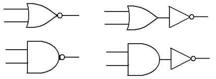
As an exercise in logic, we show
that the NAND (Not AND) gate is fundamental in that it
can be used to synthesize the AND, OR, and NOT gates. We begin with the basic NAND.
The
basic truth table for the NAND is given by
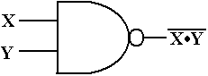 X Y X·Y
0 0 0 1
0 1 0 1
1 0 0 1
1 1 1 0
From this truth table, we see that  = 1 and
  = 0, so we
conclude that
= 0, so we
conclude that  =
= 
and immediately have the realization of the NAND gate as a NOT gate.
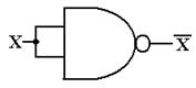
Figure: A NAND Gate Used as a NOT Gate
Here is
the AND gate as implemented from two NAND gates.
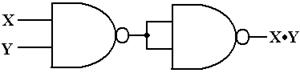
Figure: Two NAND Gates to Make an AND Gate
Notation
and DeMorgan’s Laws
We now consider two Boolean equalities that go by the name
DeMorgan’s laws, and use these
as an introduction to the notation used for negating inputs to a logic gate. DeMorgan’s laws are
often quoted in terms of set theory using the union and intersection
operators. We shall quote
these versions of the laws first and give the standard demonstration. The two laws are:

Here the symbol “Ç” denotes set
intersection, and the symbol “È” denotes set
union. Here is
the standard demonstration of these two equalities in terms of Venn diagrams.
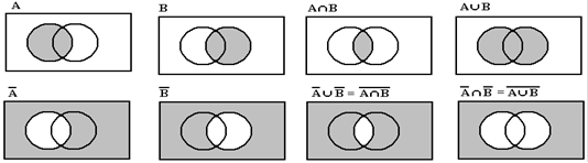
In Boolean algebra,
these laws are stated in terms of logical OR and logical AND.
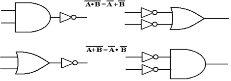
Using the
standard notation for negated inputs and outputs, these figures become the
following.
Here is a
truth–table proof of DeMorgan’s laws.
|
A
|
B
|

|

|
A + B
|
A ·
B
|

|

|

|

|
|
0
|
0
|
1
|
1
|
0
|
0
|
1
|
1
|
1
|
1
|
|
0
|
1
|
1
|
0
|
1
|
0
|
1
|
1
|
0
|
0
|
|
1
|
0
|
0
|
1
|
1
|
0
|
1
|
1
|
0
|
0
|
|
1
|
1
|
0
|
0
|
1
|
1
|
0
|
0
|
0
|
0
|
Circuits
and Truth Tables
We now address an obvious problem – how to relate circuits
to Boolean expressions.
The best way to do this is to work an example. Here is the circuit diagram to be analyzed.
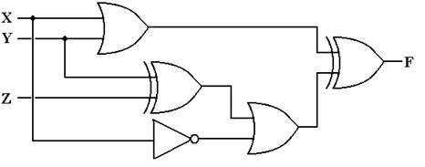
The method to get the answer is to label each gate and
determine the output of each. The
following diagram shows the gates as labeled and the output of each gate.
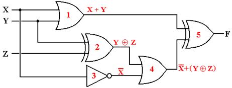
The outputs of each gate are as
follows:
The output of gate 1 is (X +
Y),
The output of gate 2 is (Y Å Z),
The output of gate 3 is X’,
The output of gate 4 is X’ +
(Y Å Z), and
The output of gate 5 is (X +
Y) Å [X’ + (Y Å Z)]
We now
produce the truth table for the function.
|
X
|
Y
|
Z
|
X + Y
|
(Y
Å Z)
|
X’
|
X’ + (Y Å Z)
|
(X
+ Y) Å [X’+(Y Å Z)]
|
|
0
|
0
|
0
|
0
|
0
|
1
|
1
|
1
|
|
0
|
0
|
10
|
0
|
1
|
1
|
1
|
1
|
|
0
|
1
|
0
|
1
|
1
|
1
|
1
|
0
|
|
0
|
1
|
1
|
1
|
0
|
1
|
1
|
0
|
|
1
|
0
|
0
|
1
|
0
|
0
|
0
|
1
|
|
1
|
0
|
1
|
1
|
1
|
0
|
1
|
0
|
|
1
|
1
|
0
|
1
|
1
|
0
|
1
|
0
|
|
1
|
1
|
1
|
1
|
0
|
0
|
0
|
1
|
Some Boolean algebra can simplify this to F(X, Y, Z) = X’·Y’ + Y’·Z’
+ X·Y·Z.
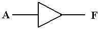
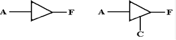
The Non–Inverting Buffer
We now investigate a number of
circuit elements that do not directly implement Boolean
functions. The first is the
non–inverting buffer, which is denoted by the following symbol.
Logically, a buffer does nothing. Electrically, the buffer serves as an
amplifier converting a
degraded signal into a more useable form; specifically it does the following in
TTL.
A logic 1
(voltage in the range 2.0 – 5.0 volts) will be output as 5.0 volts.
A logic 0 (voltage in the
range 0.0 – 0.8 volts) will be output as 0.0 volts.
While one might consider this as an amplifier, it is better
considered as a “voltage adjuster”.
We shall see another use of this and similar circuits when we consider MSI
(Medium Scale
Integrated) circuits in a future chapter.
Tri–State
Buffers
We have now seen all of the logic gates to be used in this
course. There is one more gate
type that needs to be examined – the tri-state
buffer. We begin with the
examination of a
simple (non-inverting buffer) and comment on its function. We discuss two basic types:
enabled–high and enabled–low. The
circuit diagrams for these are shown below.
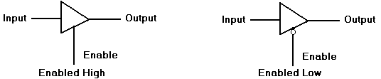
The
difference between these two circuits relates to how the circuits are
enabled. Note that
the enabled-low tri–state buffer shows the standard use of the NOT dot on
input.
The following figure shows two ways of implementing an
Enabled–Low Tri-State buffer,
one using an Enabled-High Tri-State with a NOT gate on the Enable line. The significance
of the over–bar on the Enable input is that the gate is active when the control
is logic 0.
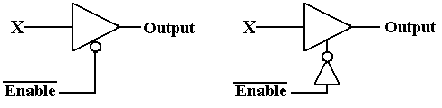
Figure: Two Views of an Enabled-Low Tri-State Buffer
A tri-state buffer acts as a simple buffer when it is
enabled; it passes the input through while
adjusting its voltage to be closer to the standard. When the tri-state buffer is not enabled, it
acts as a break in the circuit or an open switch (if you understand the
terminology). A gate
may be enabled high (C = 1) or enabled low (C = 0). Consider an enabled–high tri-state.
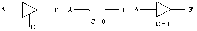
Figure: Circuits Equivalent to an Enabled Tri–State and a
Disabled Tri-State
When the enable signal is C = 1, the tri-state acts as a
simple buffer and asserts its input as an
output. When the enable signal is C = 0,
the tri-state does not assert anything on the output.
The
Third State
The definition of this “third state” in a tri–state buffer
is both obvious and subtle. Compare
the two circuits in the figure below.
One is a buffer; the other is a tri–state buffer.
For the circuit on the left, either
F = 0 (0 volts) or F = 1 (5 volts).
There is no other option.
For the circuit on the right, when C = 1 then F = A, and takes a value of
either 0 volts or 5
volts, depending on the value of the input.
When C = 0, F is simply not defined.
One of
the better ways to understand the tri-state buffer is to consider the following
circuit with
two Boolean inputs A and B, one output F, and an enable signal C.
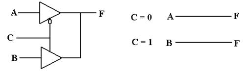
Note that the two tri–state buffers are enabled differently,
so that the top buffer is enabled if
and only if the bottom buffer is not enabled, and vice versa. The design insures that at no
time are both of the tri–state buffers enabled, so that there is no conflict of
voltages.
C = 0 Only the top buffer is enabled F = A
C = 1 Only the bottom buffer is enabled F = B
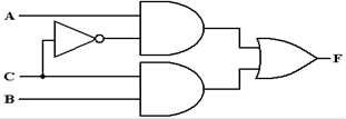
The reader will note that the above circuit is logically
equivalent to the one that follows.
Given only this simple example, one might reasonably
question the utility of tri–state buffers.
It appears that they offer a novel and complex solution to a simple
problem. The real use of
these buffers lies in placing additional devices on a common bus, a situation
in which the use
of larger OR gates might prove difficult.
Multiplexers – The Data Selectors
We
now turn to a circuit element that allows the selection of one of its inputs to
be passed on to
the
output. This is called the multiplexer. One common multiplexer would be the 8–to–1
multiplexer,
which will output one of the eight inputs, as selected by the control
logic. A
multiplexer,
also called a “MUX”, is a sample of
a small scale integrated circuit.
Typically of
many
such circuits, the MUX could easily be fabricated from more basic gates; indeed
our
discussion
will show the basic circuitry. In actual
practice though, the MUX is treated as a
single
circuit element.
A multiplexer has a number of inputs (usually a
power of two), a number of control signals, and
one output. A
demultiplexer has one input signal, a number of control signals, and a number
of
outputs, also usually a power of two. We consider here a 2N–to–1
multiplexer and a 1–to–2N
demultiplexer.
Circuit Inputs Control
Signals Outputs
Multiplexer 2N N 1
Demultiplexer 1 N 2N
Specific numbers for each of the multiplexers and
demultiplexers are given in the table
below, which is indexed by the number of control signals to each device.
|
|
Multiplexer
|
Demultiplexer
|
|
Control Signals
|
Inputs
|
Outputs
|
Inputs
|
Outputs
|
|
1
|
2
|
1
|
1
|
2
|
|
2
|
4
|
1
|
1
|
4
|
|
3
|
8
|
1
|
1
|
8
|
|
4
|
16
|
1
|
1
|
16
|
|
5
|
32
|
1
|
1
|
32
|
Multiplexers are quite useful in connecting a number of inputs to a
single output. Quite
often, the output of a multiplexer will be fed through a tri–state buffer, so
that there is the
additional option of not placing anything on the bus.
Demultiplexers are interesting, but of less use to
us at the moment.
The action of each of these circuits is determined
by the control signals. For a
multiplexer, the
output is the selected input. In a demultiplexer, the input is routed to
the selected output. As
examples, we show the diagrams for both a four–to–one
multiplexer (MUX) and a
one–to–four demultiplexer (DEMUX).
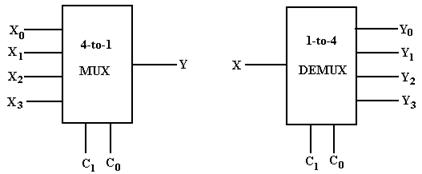
Note that each of the circuits has two control
signals. For a multiplexer, the N
control signals
select which of the 2N inputs will be
passed to the output. For a demultiplexer,
the N control
signals select which of the 2N outputs
will be connected to the input.
In this diagram, we examine the construction of a
typical 4–to–1 multiplexer from basic gates.
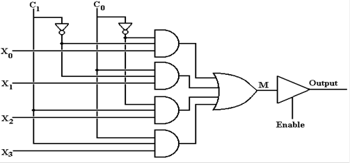
When the tri–state buffer is enabled, the output of
this circuit is determined by the selected input.
|
C1
|
C0
|
Output
|
|
0
|
0
|
X0
|
|
0
|
1
|
X1
|
|
1
|
0
|
X2
|
|
1
|
1
|
X3
|
One can also view the output, equivalently M, as a Boolean
expression.

When the tri–state is not enabled, the output, M,
of the multiplexer is not connected to the output
of the circuit.
This is likely connected to a common bus line, which can have its input
specified
by a number of sources.
Decoders
An N–to–2N decoder takes
an N bit binary code and activating the output labeled with the
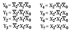
corresponding number. Consider a 3–to–8 decoder with outputs
labeled Z0, Z1, …, Z7.
Suppose the input is I3 = 1,
I2 = 0, I1 = 0, and I0 = 1 for the binary code
101. Then output Z5 is
active and the other outputs are not
active.
With one common exception, we have
only N–to–2N decoders. This
one exception is the
4–to–10 decoder. Note that it takes 4
bits to encode 10 items, as 3 bits will encode only 8. This
author’s preference would be to use a
4–to–16 decoder and ignore some of the outputs, but this
author does not establish commercial
practice. The main advantage is that the
4–to–10 decoder
chip would have 6 fewer pins than a
4–to–16 decoder; a 16–pin chip is standard and cheaper to
manufacture than a 22–pin chip.
Another issue is whether the
signals are active high or active low. Our first example has been
constructed for active high
circuits. Consider the 3–to–8 decoder as
an example. If the input
code is 101, then the output Z5
is a logic 1 (+5 volts) and all other outputs are logic 0 (0 volts).
This approach is active high. We shall handle the more realistic active low
on the next page.
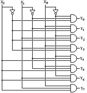
All decoders are based on the
association of binary numbers to decimal numbers. Since this is a
3–to–8 decoder, we have three inputs, labeled X2, X1,
and X0; and eight outputs, labeled Y7,
Y6, Y5, Y4, Y3, Y2, Y1,
and Y0. The observation that
leads to the design of the decoder is the
obvious one that the values of X2, X1, and X0
determine the output selected. The
following
Boolean equations determine this 3–to–8 decoder.
Here is the circuit diagram for the 3–to–8 active–high
decoder.
The Enable Input
We now
consider another important input to the decoder chip. This is the enable input. If the
decoder enable signal is active high, then the decoder is active when enable is
1 and not active
when enable = 0. We shall consider
enabled–high decoders just for the moment.
The enable
input allows the decoder to be either enabled or disabled. For an active high decoder that is
enabled high (Enable = 1 activates it) we have the following.
Enable = 0 All outputs of the decoder are 0
Enable = 1 The selected output of the decoder is 1,
all other outputs are 0.
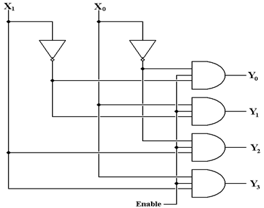
The action of the above decoder is described in the
following truth table.
|
Enable
|
X1
|
X0
|
Y0
|
Y1
|
Y2
|
Y3
|
|
0
|
d
|
d
|
0
|
0
|
0
|
0
|
|
1
|
0
|
0
|
1
|
0
|
0
|
0
|
|
1
|
0
|
1
|
0
|
1
|
0
|
0
|
|
1
|
1
|
0
|
0
|
0
|
1
|
0
|
|
1
|
1
|
1
|
0
|
0
|
0
|
1
|
The top row in the above truth table has “d” as an entry for both X1
and X0. Each of these
entries is read as “don’t care”, indicating that when Enable = 0, all outputs
are 0 without
regard to the values of the two inputs, X1 and X0.
In real
commercial circuits, we often have outputs as active low, in which case the
above decoder
would have output Z5 as a logic 0 (0 volts) and all other outputs as
logic 1 (+5 volts). The truth
table of a 2–to–4 commercial decoder would be as follows.
|
Enable#
|
X1
|
X0
|
Y0
|
Y1
|
Y2
|
Y3
|
|
1
|
d
|
d
|
1
|
1
|
1
|
1
|
|
0
|
0
|
0
|
0
|
1
|
1
|
1
|
|
0
|
0
|
1
|
1
|
0
|
1
|
1
|
|
0
|
1
|
0
|
1
|
1
|
0
|
1
|
|
0
|
1
|
1
|
1
|
1
|
1
|
0
|
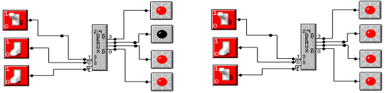
The following is a screen shot from the circuit emulator used in
association with this course. The
diagram on the left has E# = 0, so that X1 = 1 and X0 = 0
causes the output Y2 to be asserted low.
When E# = 1, none of the outputs are asserted low; all are at logic high.
There are two standard approaches to building an
enabled–low, active–low decoder. The
next
figure shows both of them. The circuit
on the left resembles the one in Rob Williams’s book; the
one on the right can be shown by simple Boolean algebra to be equivalent.
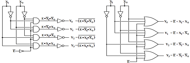
There are a few commercial practices reflected in
the circuit on page 85 of the textbook by Rob
Williams. Your author will comment on
these now. The first is the use of NAND
gates, rather
than the equivalent AND gates followed by NOT gates. By definition NAND is NOT AND. In
terms of basic electronics, the NAND gate is simpler and faster than the AND
gate, hence it is
much faster than a two gate combination of AND followed by NOT. Your author’s circuit above
to the left is designed that way to make the logic clear.
The second has to do with the double NOTs on the
inputs. Consider the 3–to–8 version of
the
decoder above to the left and look at one of the input lines.

The diagram to the left shows what the input would
be for a 3–to–8 version of the above
decoder. Each input would drive five
gates, four AND gates directly and one NOT gate.
The circuit on the right follows commercial practice, each input drives only
one gate. The cost
of this design modification is that there are two NOT gates, the first
producing NOT(X) and the
second one producing X again. It has
been the commercial experience that it is preferable to
limit the number of gates driven by any one input; the count of one is the
minimum.
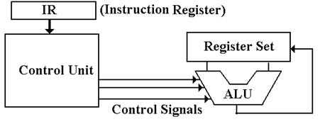
The Control Unit
The control unit is the central subsystem in any
computer. It functions to interpret the
binary
machine language and cause the computer to execute the indicated instructions. As input, the
control unit has the contents of the IR (Instruction Register), the system
clock, and status bits
from the ALU indicating the results of the last computation.
The control unit is one of the four major components
of the CPU (Central Processing Unit). It
issues control signals to the ALU, the datapath (placing data on CPU busses,
and routing the
ALU output to its destination), the memory, and all I/O units. The internal structure of the CPU,
with the control unit, is shown below.
The one critical design decision here is how to
generate the control signals. We know
the inputs,
we know the rules to follow, and we know what the outputs must be. But, how are these outputs
to be generated from the inputs and state?
There are two primary ways to do this.
All modern stored program computers
execute programs that are a sequence of binary machine–
language instructions. This sequence of
instructions are translations of either an assembly
language program or a program in a higher–level language, such as C++ or Java. Each
instruction to be executed is fetched from memory and deposited in the Instruction Register,
which is a part of the control unit. The
control unit interprets this machine instruction and
issues the signals that cause the computer to execute it.
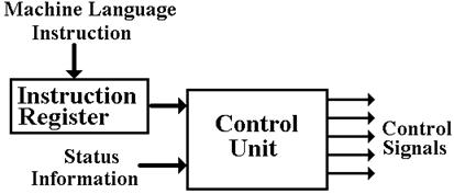
Figure: Schematic of the Control
Unit
There are two ways in which a
control unit may be organized. The most
efficient way is to build
the unit entirely from basic logic gates (AND, OR, NOT, and Exclusive OR). For a moderately–
sized instruction set with the standard features expected, this leads to a very
complex circuit that
is difficult to test.
In 1951, Maurice V. Wilkes (designer
of the EDSAC, see above) suggested an organization for
the control unit that was simpler, more flexible, and much easier to test and
validate. This was
called a “microprogrammed control unit”. The basic idea was that control signals can
be
generated by reading words from a micromemory
and placing each in an output buffer.
In this design, the control unit
interprets the machine language instruction and branches to a
section of the micromemory that contains the microcode needed to emit the proper control
signals. The entire contents of the
micromemory, representing the sequence of control signals
for all of the machine language instructions is called the microprogram. All we need to
know is
that the microprogram is stored in a ROM (Read Only Memory) unit.
While microprogramming was
sporadically investigated in the 1950’s, it was not until about
1960 that memory technology had matured sufficiently to allow commercial
fabrication of a
micromemory with sufficient speed and reliability to be competitive. When IBM selected the
technology for the control units of some of the System/360 line, its primary
goal was the creation
of a unit that was easily tested. Then
they got a bonus; they realized that adding the appropriate
blocks of microcode could make a S/360 computer execute machine code for either
the IBM
1401 or IBM 7094 with no modification.
This greatly facilitated upgrading from those machines
and significantly contributed to the popularity of the S/360 family, as many of
their commercial
customers had a very large installed base of machine code and did not want to
change.
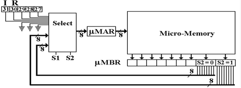
Here is the design for a typical
microprogrammed control unit. This functions
by copying one
micro–word at a time from the micromemory, also called the CROM (Control ROM)
into a set
of registers that actually emit the control signals. The only function of the Select circuitry is
to
select the address of the next micro–word to be read.
The microcoded (or microprogrammed)
control unit shows its utility in the management of
virtual memory, which we shall consider in Chapter 12. The processes for this management
are quite easy to describe in coding terms, but hard to imagine in terms of
pure digital gates.
Microprogramming became quite
popular as a design tool in the 1970’s and remained popular
through the 1980’s and into the early 1990’s.
It is still used today, though in moderation with
somewhat less enthusiasm than before.
The use of microcoding allowed the
management of very complex assembly language
instructions by a fairly simple, and easily tested, control unit. As a result, the instruction sets
of computers of the time became quite complex, leading to some designs being
classified as
CISC (Complex Instruction Set Computers). The primary
example of CISC was the VAX,
developed by the Digital Equipment Corporation in the late 1970’s.
Reduced
Instruction Set Computers
The acronym RISC stands for “Reduced Instruction
Set Computer”. RISC
represents a design
philosophy for the ISA (Instruction Set Architecture) and the CPU
microarchitecture that
implements that ISA. RISC is not a set
of rules; there is no “pure RISC” design.
The acronym
CISC, standing for “Complex Instruction Set Computer”,
is a term applied by the proponents
of RISC to computers that do not follow that design.
The first designed called “RISC” date to the early
1980’s. The movement began with two
experimental designs, the IBM 801 in 1980 and the RISC 1, developed by UC
Berkeley in 1981.
We should note that the original RISC machine was
probably the CDC–6400 designed and built
by Mr. Seymour Cray, then of the Control Data Corporation. In designing a CPU that was
simple and very fast, Mr. Cray applied many of the techniques that would later
be called “RISC”
without himself using the term.
Why
CISC?
Early CPU designs could have followed the RISC
philosophy, the advantages of which were
apparent early. Why then was the CISC
design followed? Here are two reasons:
1. CISC
designs make more efficient use of memory. In particular, the “code density” is better,
more instructions per kilobyte. After
all, memory was very expensive and prone to failure.
In 1973, memory costs were about $400,000 per megabyte, and the average memory
size was
on the order of 8 to 32 KB.
2. CISC
designs close the “semantic gap”; they produce an ISA with instructions that
more closely resemble those in a higher–level language. This should provide
better
support for the compilers.
The two assumptions above are no longer true. Beginning with the use of VLSI for memory
chips in the late 1980’s, memory prices began to drop, from $2,000 per megabyte
in 1983 to
less than $50 per gigabyte in 2010.
The second reason did not hold up to experimental
scrutiny. While it was thought that more
complex assembly languages would provide better support for compilers, it was
discovered that
compilers did not use those complex features.
Beginning in the early 1980’s, computer designers
began to suspect that simpler instruction set
architectures would lead to simpler and faster control units, hence to faster
computers. This was
the beginning of the RISC movement. The
basic RISC principle: “A simpler CPU is a faster CPU”.
A number of the more common strategies include:
1) Fixed instruction length, generally one
word. This simplifies instruction fetch.
2) Simplified addressing modes.
3) Fewer and simpler instructions in the
instruction set.
4) Only load and store instructions access
memory; no add memory to register, add
memory to memory, etc. Memory access is the slow part of
computation, so limiting
such access will speed up the
computer.
5) Let the compiler do it. Use a good compiler to break complex
high-level language
statements into a number of
simple assembly language statements.
As indicated above, the primary noticeable
difference between a RISC design and a CISC
design will be found in the structure of the assembly language. The easiest way to illustrate
this difference is to examine the handling of a single (fairly silly) Java
statement by each of
the two designs. The Java statement is
as follows.
x[k++] = y[m++] + z[n++] ; // Don’t ask what this does.
By assumption, this single statement is posited to
be equivalent to the following block of code.
x[k] = y[m] + z[n] ;
k = k + 1 ;
m = m + 1 ;
n = n + 1 ;
Most compilers for the VAX–11/780 would compile the
above statement into one VAX
assembly language instruction, which could handle both the addition and the
adjustment of
all three array indices. Of course,
there was no Java compiler in 1980.
A less conventional CISC design might compile the
first Java statement into four lines of
assembly language, one for each of the Java lines in the equivalent code block.
Most modern RISC machines are load/store devices, in
which arithmetic operations are done
only on values in registers and never directly on memory addresses. What now follows is
pseudo–Pentium assembly language, written in the style of a load/store RISC
machine. This
uses two registers, EAX and EBX, that are true 32–bit Pentium registers.
LOAD
EAX, Y[M]
LOAD
EBX, Z[N]
ADD
EAX, EBX // EAX GETS THE SUM
STORE EAX, Z[K]
LOAD
EAX, K
INC
EAX // EAX IS INCREMENTED
BY 1
STORE EAX, K // K++
LOAD
EAX, M
INC
EAX
STORE EAX, M // M++
LOAD
EAX, N
INC
EAX
STORE EAX, N // N++
What might take one very complex VAX assembly language instruction takes
13 instructions
on our hypothetical, but realistic, load/store RISC design. This is one consideration to keep in
mind when comparing execution rates of RISC and CISC designs. It is true that the RISC
design will execute more instructions per second that the CISC design, but each
RISC
instruction does less work than the CISC instruction. What is the total work per unit time?