Of course, there is no such thing as a pure Read-Only
memory; at some time it must be possible
to put data in the memory by writing to it, otherwise there will be no data in
the memory to be
read. The term “Read-Only” usually
refers to the method for access by the CPU.
All variants of
ROM share the feature that their contents cannot be changed by normal CPU write
operations.
All variants of RAM (really Read-Write Memory) share the feature that their
contents can be
changed by normal CPU write operations.
Some forms of ROM have their contents set at time
of manufacture, other types called PROM
(Programmable ROM), can have contents changed by
special devices called PROM Programmers.
Pure ROM is more commonly found in devices, such as
keyboards, that are manufactured in
volume, where the cost of developing the chip can be amortized over a large
production volume.
PROM, like ROM, can be programmed only once.
PROM is cheaper than ROM for small
production runs, and provides considerable flexibility for design. There are several varieties
of EPROM (Erasable PROM), in which
the contents can be erased and rewritten many times.
There are very handy for research and development for a product that will
eventually be
manufactured with a PROM, in that they allow for quick design changes.
We now introduce a new term, “shadow RAM”. This is an old
concept, going back to the early
days of MS–DOS (say, the 1980’s). Most
computers have special code hardwired into ROM.
This includes the BIOS (Basic Input / Output System), some device handlers, and
the start–up, or
“boot” code. Use of code directly from
the ROM introduces a performance penalty, as ROM
(access time about 125 to 250 nanoseconds) is usually slower than RAM (access
time 60 to 100
nanoseconds). As a part of the start–up
process, the ROM code is copied into a special area of
RAM, called the shadow RAM, as it
shadows the ROM code. The original ROM
code is not
used again until the machine is restarted.
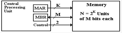
The Memory Bus
The
Central Processing Unit (CPU) is connected to the memory by a high–speed
dedicated
point–to–point bus. All memory busses
have the following lines in common:
1. Control lines. There are at least two, as mentioned in Chapter
3 of these notes.
The Select# signal is asserted low to activate the memory and the R/W# signal
indicates the operation if the
memory unit is activated.
2. Address lines. A modern computer will have either 32 or 64
address lines on the
memory bus, corresponding to
the largest memory that the design will accommodate.
3. Data Lines. This is a number of lines with data bits
either being written to the memory
or being read from it. There will be at least 8 data lines to allow
transfer of one byte at
a time. Many modern busses have a “data bus width” of 64 bits; they can
transfer eight
bytes or 64 bits at one
time. This feature supports cache
memory, which is to be
discussed more fully in a
future chapter of this text.
4. Bus clock. If present, this signal makes the bus to be a
synchronous bus. Busses
without clock signals are asynchronous busses. There is a special class of RAM
designed to function with a
synchronous bus. We investigate this
very soon.
Modern
computers use a synchronous memory bus, operating at 133 MHz or higher. The bus
clock frequency is usually a fraction of the system bus; say a 250 MHz memory
bus clock
derived from a 2 GHz (2,000 MHz) system clock.
Memory Registers
Memory
is connected through the memory bus to the CPU via two main registers, the MAR
(Memory Address Register) and
the MBR (Memory Buffer Register). The latter register is
often called the MDR (Memory Data Register). The number of bits in the MAR matches the
number of address lines on the memory bus, and the number of bits in the MBR
matches the
number of data lines on the memory bus.
These registers should be considered as the CPU’s
interface to the memory bus; they are logically part of the CPU.
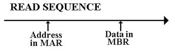
Memory Timings
There
are two ways to specify memory speed: access time and the memory clock
speed. We
define each, though the access time measure is less used these days. Basically the two measures
convey the same information and can be converted one to the other. The memory access time is
defined in terms of reading data from the memory. It is the time between the address
becoming stable in the MAR and the data becoming available in the MBR. In modern memories
this time can range from 5 nanoseconds (billionths of a second) to 150
nanoseconds, depending
on the technology used to implement the memory.
More on this will be said very soon.
When
the memory speed is specified in terms of the memory clock speed, it implies an
upper
limit to the effective memory access time.
The speed of a modern memory bus is usually
quoted in MHz (megahertz), as in 167 MHz. The actual unit is inverse seconds (sec–1),
so
that 167 MHz might be read as “167 million per second”. The bus clock period is the inverse
of its frequency; in this case we have a frequency of 1.67·108 sec–1,
for a clock period of
t = 1.0 / (1.67·108 sec–1)
= 0.6·10–8
sec = 6.0 nanoseconds.
Memory Control
Just
to be complete, here are the values for the two memory control signals.
|
Select# |
R/W# |
Action |
|
1 |
0 |
Memory
contents are not changed |
|
1 |
1 |
|
|
0 |
0 |
CPU
writes data to the memory. |
|
0 |
1 |
CPU
reads data from the memory. |
Registers and
Flip–Flops
One
basic division of memory that is occasionally useful is the distinction between
registers and
memory. Each stores data; the basic
difference lies in the logical association with the CPU.
Most registers are considered to be part of the CPU, and the CPU has only a few
dozen registers.
Memory is considered as separate from the CPU, even if some memory is often
placed on the
CPU chip. The real difference is seen in
how assembly language handles each of the two.
Although we have yet to give a formal definition of a
flip–flop, we can now give an intuitive
one.
A flip–flop is a “bit box”; it stores a single binary bit. By Q(t), we denote the state of the
flip–flop at the present time, or present
tick of the clock; either Q(t) = 0 or Q(t) = 1.
The student
will note that throughout this
textbook we make the assumption that all circuit elements function
correctly, so that any binary device
is assumed to have only two states.
A flip–flop must have an output; this is called either Q or
Q(t). This output indicates the current
state of the flip–flop, and as such
is either a binary 0 or a binary 1. We
shall see that, as a result
of the way in which they are
constructed, all flip–flops also output![]() , the complement of the
, the complement of the
current state. Each flip–flop also has, as input, signals
that specify how the next state, Q(t + 1),
is to relate to the present state,
Q(t). The flip–flop is a synchronous
sequential circuit element.
The Clock
The most fundamental characteristic
of synchronous sequential circuits is a system clock. This is
an electronic circuit that produces
a repetitive train of logic 1 and logic 0 at a regular rate, called
the clock frequency. Most
computer systems have a number of clocks, usually operating at
related frequencies; for example – 2
GHz, 1GHz, 500MHz, and 125MHz. The
inverse of the
clock frequency is the clock cycle time. As an example, we consider a clock with a
frequency
of 2 GHz (2·109 Hertz).
The cycle time is 1.0 / (2·109) seconds, or
0.5·10–9 seconds = 0.500
nanoseconds = 500 picoseconds.
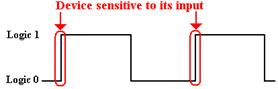
Synchronous sequential circuits are sequential circuits that use a clock input to
order events.
The following figure illustrates
some of the terms commonly used for a clock.
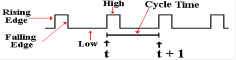
The clock input is very important to the concept of a
sequential circuit. At each “tick” of
the
clock the output of a sequential
circuit is determined by its input and by its state. We now
provide a common definition of a “clock
tick” – it occurs at the rising edge of each pulse. By
definition, a flip–flop is sensitive to its input only on the rising edge of
the system clock.
There are four
primary types of flip–flop: SR (Set Reset), JK, D (Data) and T (Toggle). We
concern ourselves with only two: the D and the T. The D flip–flop just stores whatever input
it had at the last clock pulse sent to it.
Here is one standard representation of a D flip–flop.
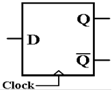 When D = 0 is
sampled at the rising edge of the clock,
When D = 0 is
sampled at the rising edge of the clock,
the value Q will be 0 at the next clock pulse.
When D = 1 is
sampled at the rising edge of the clock,
the value Q will be 1 at the next clock pulse.
This D flip–flop
just stores a datum.
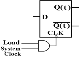 The next
question is how to prevent this device
The next
question is how to prevent this device
from loading a new value on the rising edge of
each system clock pulse. We want it to
store a
value until it is explicitly loaded with a new one.
The answer is to
provide an explicit load signal,
which allows the system clock to influence the
flip–flop only when it is asserted.
It should be
obvious that the control unit must
synchronize this load signal with the clock.
The T
flip–flop is one that retains its state when T = 0 and changes it when T =
1.
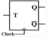 Here is the
standard circuit diagram for a T flip–flop.
Here is the
standard circuit diagram for a T flip–flop.
When T = 0 is
sampled at the rising edge of the clock,
the value Q will remain the same; Q(t + 1) = Q(t).
When T = 1 is
sampled at the rising edge of the clock,
the value Q will change; Q(t + 1) = NOT (Q(t)).
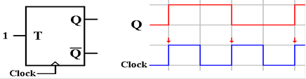
In this circuit,
the input is kept at T = 1. This causes
the value of the output to change at
every rising edge of the clock. This
causes the output to resemble the system clock, but at
half of the frequency. This circuit is a
frequency divider.
The next circuit
suggests the general strategy for a frequency divider.
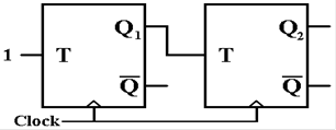 The circuit at
left shows two T flip–flops, in
The circuit at
left shows two T flip–flops, in
which the output of T1 is the input to T2.
When the output
of T1 goes high, T2 changes
at the rise of the next clock pulse.
Here is the
timing for this circuit.
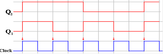
Note that Q1
is a clock signal at half the frequency of the system clock, and Q2
is another
clock signal at one quarter the frequency of the system clock. This can be extended to produce
frequency division by any power of two.
Frequency division by other integer values can be
achieved by variants of shift registers, not studied in this course.
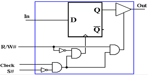
The Basic Memory Unit
All
computer memory is ultimately fabricated from basic memory units. Each of these devices
stores one binary bit. A register to
store an 8–bit byte will have eight basic units. Here is a
somewhat simplified block diagram of a basic memory unit.
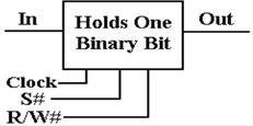 There are two
data lines: Input (a bit to be stored in the
There are two
data lines: Input (a bit to be stored in the
memory) and Output (a bit read from the memory).
There
are two basic control lines. S# is
asserted low to
select the unit, and R/W# indicates whether it is to be read
or written to. The Clock is added to be
complete.
At
present, there are three technologies available for main RAM. These are magnetic core
memory, static RAM (SRAM) and dynamic RAM (DRAM). Magnetic core memory was much
used from the mid 1950’s through the 1980’s, slowly being replaced by
semiconductor memory,
of which SRAM and DRAM are the primary examples.
At
present, magnetic core memory is considered obsolete, though it may be making a
comeback
as MRAM (Magnetic RAM). Recent product
offerings appear promising, though not cost
competitive with semiconductor memory.
For the moment, the only echo of magnetic core
memory is the occasional tendency to call primary memory “core memory”
Here
is a timing diagram for such a memory cell, showing a write to memory, followed
by an
idle cycle, then a read from memory.
Note the relative timings of the two control signals S#
and R/W#. The important point is that
each has its proper value at the rising edge of the clock.
Here they are shown changing values at some vague time before the clock rising
edge.
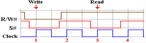
At
the rising edge of clock pulse 1, we have R/W# = 0 (indicating a write to
memory) and
S# = 0 (indicating the memory unit is selected). The memory is written at clock pulse 1.
At
the rising edge of clock pulse 2, S# = 1 and the memory is inactive. The value of R/W#
is not important as the memory is not doing anything.
At
the rising edge of clock pulse 3, R/W# = 1 (indicating a read from memory) and
S# = 0.
The memory is read and the value sent to another device, possibly the CPU.
As
indicated above, there are two primary variants of semiconductor read/write
memory. The
first to be considered is SRAM (Static RAM) in which the basic memory cell is
essentially a
D flip–flop. The control of this unit
uses the conventions of the above timing diagram.
When
S# = 1, the memory unit is not active.
It has a present state, holding one bit.
That bit
value (0 or 1) is maintained, but is not read.
The unit is disconnected from the output line.
When
S# = 0 and R/W# = 0, the flip–flop is loaded on the rising edge of the
clock. Note that
the input to the flip–flop is always attached to whatever bus line that
provides the input. This
input is stored only when the control signals indicate.
When
S# = 0 and R/W# = 1, the flip–flop is connected to the output when the clock is
high.
The value is transferred to whatever bus connects the memory unit to the other
units.
The
Physical View of Memory
We now examine two design choices that produce
easy-to-manufacture solutions that offer
acceptable performance at reasonable price.
The basic performance of DRAM chips has not
changed since the early 1990s’; the basic access time is in the 50 to 80
nanosecond range, with
70 nanoseconds being typical. The first
design option is to change the structure of the main
DRAM memory. We shall note a few design
ideas that can lead to a much faster memory.
The second design option is to build a memory hierarchy, using various levels
of cache memory,
offering faster access to main memory.
As mentioned above, the cache memory will be faster
SRAM, while the main memory will be slower DRAM.
In a multi–level memory that uses
cache memory, the goal in designing the primary memory is
to have a design that keeps up with the cache closest to it, and not
necessarily the CPU. All
modern computer memory is built from a collection of memory chips. These chips are usually
organized into modules. In a
byte–addressable memory, each memory module will have eight
memory chips, for reasons to be explained. The use of memory modules allows an
efficiency boost due to the process called “memory interleaving”.
Suppose a computer with
byte-addressable memory, a 32–bit address space, and 256 MB
(228 bytes) of memory. Such a
computer is based on this author’s personal computer, with the
memory size altered to a power of 2 to make for an easier example. The addresses in the MAR
can be viewed as 32–bit unsigned integers, with high order bit A31
and low order bit A0. Putting
aside issues of virtual addressing (important for operating systems), we
specify that only
28–bit addresses are valid and thus a valid address has the following form.
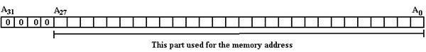
The memory of all modern computers comprises a number of modules,
which are combined to
cover the range of acceptable addresses.
Suppose, in our example, that the basic memory chips
are 4Mb (megabit) chips, grouped to form 4MB modules. The 256 MB memory would be built
from 64 modules and the address space divided as follows:
6 bits to select the memory module
as 26 = 64, and
22 bits to select the byte within
the module as 222 = 4·220 = 4M.
The question is which bits select
the module and which are sent to the module.
Two options
commonly used are high-order memory
interleaving and low-order memory
interleaving.
Other options exist, but the resulting designs would be truly bizarre. We shall consider only
low-order memory interleaving in which the low-order address bits are used to
select the
module and the higher-order bits select the byte within the module. The advantage of
low–order interleaving over high–order interleaving will be seen when we consider
the
principle of locality. Memory tends to
be accessed sequentially by address.
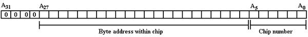
This low-order interleaving has a number of
performance-related advantages. These
are due to
the fact that consecutive bytes are stored in different modules, thus byte 0 is
in chip 0,
byte 1 is in chip 1, etc. In our example
Module 0 contains bytes 0, 64, 128, 192, etc., and
Module 1 contains bytes 1, 65, 129, 193, etc., and
Module 63 contains bytes 63, 127, 191, 255, etc.
Suppose that the computer has a 64
bit–data bus from the memory to the CPU.
With the above
low-order interleaved memory it would be possible to read or write eight bytes
at a time, thus
giving rise to a memory that is close to 8 times faster. Note that there are two constraints on the
memory performance increase for such an arrangement.
1) The
number of chips in the memory – here it is 64.
2) The
width of the data bus – here it is 8, or 64 bits.
In this design, the chip count matches the bus width; it is a balanced design.
To anticipate a later discussion,
consider the above memory as connected to a cache memory that
transfers data to and from the main memory in 64–bit blocks. When the CPU first accesses an
address, all of the words (bytes, for a byte addressable memory) in that block
are copied into the
cache. Given the fact that there is a
64–bit data bus between the main DRAM and the cache, the
cache can be very efficiently loaded. We
shall have a great deal to say about cache memory later
in this chapter.
There is a significant speed advantage to low–order
interleaving that is best illustrated with
a smaller number of memory modules.
Consider the above scheme, but with an eight–way
low–order interleaved memory. The memory
modules are identified by the low–order three
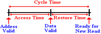
bits of the address: A2, A1, A0. The modules can be numbered 0 through 7. Suppose that the
memory is fabricated from chips with 80 nanosecond cycle time. Unlike the access time, which
measures the delay from the address assertion to the data being loaded in the
data buffer, the
cycle time represents the minimum
time between independent accesses to the memory. The
cycle time has two major components: access time and recharge time. The recharge time
represents the time required to reset the memory after a read operation. The precise meaning
of this will become clear when we discuss DRAM.
Here is a timeline showing the access time and cycle time
for a DRAM element. Here, the
timings are specified for memory READ operations.
Suppose that this is an 8–chip module with the 80 nanosecond
cycle time. The maximum
data rate for reading memory would be one byte every 80 nanoseconds. In terms of frequency
this would connect to a 12.5 MHz data bus.
Recall that even a slow CPU (2 GHz) can issue
one memory READ request every nanosecond.
This memory is about 80 times too slow.
We now implement the 8–way low order interleaving, using the
memory with an cycle time of
80 nanoseconds and an access time of 40 nanoseconds (a bit fast). Suppose that the CPU reads
in sequence the bytes from address 1000 through 1008. As is seen in the diagram below, the
CPU can issue a READ command every 10 nanoseconds.
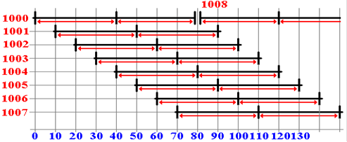
At T = 0, the CPU
issues a READ command for address 1000 in module 0.
At T = 10, the CPU
issues a READ command for address 1001 in module 1.
At T = 20, the CPU
issues a READ command for address 1002 in module 2.
At T = 30, the CPU
issues a READ command for address 1003 in module 3.
At T = 40, the CPU
issues a READ command for address 1004 in module 4.
Note that the data
for address 1000 are ready to be transferred to the CPU.
At T = 50, the CPU
issues a READ command for address 1005 in module 5.
The data for address
1001 can be transferred to the CPU.
At T = 60, the CPU
issues a READ command for address 1006 in module 6.
The data for address
1002 can be transferred to the CPU.
At T = 70, the CPU
issues a READ command for address 1007 in module 7.
The data for address
1003 can be transferred to the CPU.
At T = 80 module 0
has completed its cycle time and can accept a read from address 1008.
The data for address
1004 can be transferred to the CPU.
Here we have stumbled upon another timing issue, which we
might as well discuss now. Note
that the first value to be read is not ready for transfer until after 40
nanoseconds, the access time.
After that one value can be transferred every ten nanoseconds.
This is an example of the two measures: latency and
bandwidth. The latency for a memory is
the time delay between the first request and the first value being ready for
transfer; here it is forty
nanoseconds. The bandwidth represents the transfer rate, once the steady state
transfer has
begun. For this byte–addressable memory,
the bandwidth would be one byte every ten
nanoseconds, or 100 MB per second.
Low–order memory interleaving was one of the earliest tricks
to be tried in order to increase
memory performance. It is not the only
trick.
Selecting
the Memory Word
In
this paragraph, we use the term “word” to indicate the smallest addressable
unit of primary
memory. For most modern computers, this
would be an eight–bit byte. We now
revisit the
mechanism by which the individual word (addressable unit) is selected.
Recall
from our discussion of data formats that an N–bit unsigned binary number can
represent
a decimal number in the range from 0 through 2N – 1 inclusive. As examples, an 8–bit unsigned
binary number can range from 0 through 255, a 12–bit can range from 0 through
4095, a 20–bit
can range from 0 through 1,048,575 (220 = 1,048,576), and a 32 bit
number from 0 through
4,294,967,295 (232 = 4,294,967,296).
Recall
also our earlier discussion of decoders.
A typical decoder is an N–to–2N device, basically
converting the unsigned binary code to its decimal equivalent. The example for this discussion
will be a 4–to–16 decoder. While rather
small, it is large enough to make the point.
When used
as a decoder for memory addresses, such a device is called an address decoder.
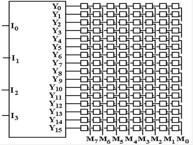
Suppose
that the 4–bit address 1011 is issued to the memory. The decoder output Y11 is
asserted and the eight memory elements associated with that address are
activated. Eight bits
are either transferred to the selected byte or read from the byte. Note that the structure of the
decoder is the reason that memory size is given in powers of 2; 1KB = 210
bytes, etc.
While
the above is a perfectly good implementation of a 16–word memory, the single
decoder scheme does not scale well.
Consider a memory that is rather small by today’s
standards. A 64MB memory would require a
26–to–67,108,864 decoder, as 64 MB =
64·1048576 bytes =
26·220
bytes = 226 bytes. While such
a decoder could be built, it would
be rather large and unacceptably slow.
Memories with fewer addressable units have smaller
address decoders, which tend to be faster.
When
we revisit SRAM in the chapter on the memory hierarchy, we shall comment on the
fact
that the cache memories tend to be small.
This is partly due to the fact that address decoding
for small memories is faster. A standard
Pentium has a split L1 cache (note error in Williams’
text on page 125), with two 16 KB caches each requiring a 14–to–16,384 decoder. As we shall
see, even this is probably implemented as two 7–to–128 decoders.
Capacitors
and DRAM
While
it is quite possible to fabricate a computer using SRAM (Static RAM, comprising
flip–flops), there are several drawbacks to such a design. The biggest problem is cost, SRAM
tends to cost more than some other options.
It is also physically bigger than DRAM, the
principle alternative. Here are the
trade–offs.
SRAM is physically bigger, more costly,
but about ten times faster.
DRAM is physically smaller, cheaper,
and slower.
Note
that memory options, such as mercury delay lines, that are bigger, more costly,
and slower
have quickly become obsolete. If the
memory is slower, it must have some other advantage
(such as being cheaper) in order to be selected for a commercial product.
We
are faced with an apparent choice that we do not care for. We can either have SRAM
(faster and more expensive) or DRAM (slower and cheaper). Fortunately, there is a design trick
that allows the design to approximate the speed of SRAM at the cost of
DRAM. This is the
trick called “cache memory”, discussed later in our chapter on the memory
hierarchy.
DRAM
(Dynamic RAM) employs a capacitor as
its key storage element. A capacitor is
a
device that stores electronic charge.
The flow of electronic charge is called “current”. There
are many uses for capacitors in alternating current circuits and radios; our
interest here is
focused on its ability to store charge.
Introductory
physics courses often discuss electric charge and current in terms borrowed
from
water flow in pipes. There is a very
familiar hydraulic analog of a capacitor; it is the tank on a
standard flush toilet. During normal
operation, the tank holds water that can be released as a
significant flow into the toilet bowl.
The tank is then slowly refilled by a current of water
through the feed lines. Another example
is seen in the electronic flashes found on most
cameras and many cell phones. The
battery charges the capacitor with a small current. When
the capacitor is charged it may be quickly discharged to illuminate the flash
bulb.
All
toilet tanks leak water; the seal on the tank is not perfect. At intervals, the float mechanism
detects the low water level and initiates a refilling operation. There is an analogous operation
for the capacitor in the DRAM; it is called “refresh” which occurs during the refresh cycle.
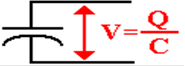
The
basic mechanism is simple. Each
capacitor can hold a charge up to a fixed maximum,
determined by a measure called its capacitance. While the charge on a capacitor is hard to
measure directly, it is easy to measure indirectly. Capacitance is defined as the charge stored
per unit voltage. If the capacitor has
capacitance C, stores a charge Q, and has a voltage V, then
C = Q/V by definition. Since the capacitance of the DRAM memory cell
is known, measuring
the voltage across the capacitor can determine the charge stored.
Since
the DRAM cell is a binary unit, there are only two values stored: 0 volts (no
charge) and
full voltage (full charge). The refresh
cycle measures the voltage across the capacitor in every
memory cell. If above a certain value,
it must have been fully charged at some point and lost its
charge. The refresh circuitry then
applies full voltage to the memory cell and brings the charge
back up to full value. Below a given
value, the charge is taken as zero, and nothing is done.
All
modern memory is implemented as a series of modules, each of which comprises
either
eight or nine memory chips of considerable capacity. Each module now has the refresh logic
built into it, so that the CPU does not need to manage the DRAM.
Another DRAM
Organization
The
apparently simple memory organization shown a few pages back calls for a single
large
decoder. As mentioned at the time, this
large decoder would present problems both in size and
time delays. One way to solve this
problem is to treat the memory as a two–dimensional array,
with row and column indices. This
reduces the problem of an N to 2N decoder to two (N/2) to
2(N/2) decoders; as in one 26–to–67,108,864 decoder vs. two
13–to–8,192 decoders.
There
is a bit of a problem with this organization, but that is easily solved. Consider the figure
presented a few pages back. It shows a
16–by–8 memory. A 64 MB memory in that
style would
be implemented as a singly dimensioned array of 67,108,864 entries of 8 bits
each. How can this
be represented as a number of square arrays, each 8,192 by 8,192, requiring two
13–to–8,192
decoders? The answer is to have a
67,108,864 byte (64MB) memory module comprising eight
67,108,864 bit (64 Mb) memory chips, along with the control circuitry required
to manage the
memory refresh. The figure below, copied
from an earlier chapter in this textbook, shows the
arrangement of such a module. Note that
there are nine chips in this module: one controller
chip and eight memory chips.
In
order to use this modular array of single bit chips, we must modify the basic
memory cell to
accept two select signals, a row select and a column select. This is done easily.
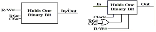
The
figure at the left shows the new logical depiction of the memory cell, with its
two
select signals. The figure at right
shows the modification of the simple memory cell to
accommodate this design. If RS# = 0 and
CS# = 0, then the cell is selected; otherwise not.
Here
is a diagram of a 16–bit memory array, organized in the two–dimensional
structure. Note
that the R/W# and memory cell I/O lines have been omitted for the sake of
clarity.
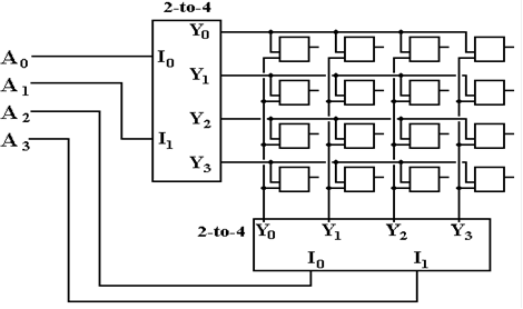
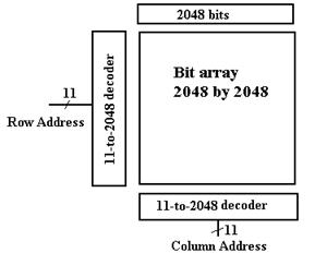
Imagine
a 4 MB (megabyte) memory module. It
would hold eight 4 Mb (megabit) memory
chips, each organized as a 2,048 by 2,048 array of single bits. Note the 2048 bit array at the
top of the square array. This will be
explained shortly. There are two
11–to–2048 decoders.
We
now come to a standard modification that at first seems to be a step back. After describing
this modification, we show that it does not lead to a decrease in memory
performance. The
modification is a result of an attempt to reduce the pin count of the memory
chip.
Each
chip is attached to a mounting board through a series of pins. For a memory chip, there
would be one pin for the bit input/output, pins for the address lines, pins for
the power and
ground lines, and pins for the control lines.
Consider
now the two–dimensional memory mentioned above.
What pins are needed?
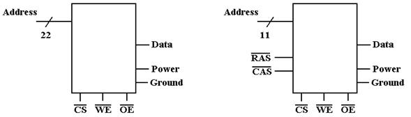
Pin Count
Address Lines 22 Address
Lines 11
Row/Column 0 Row/Column 2
Power & Ground 2 Power
& Ground 2
Data 1 Data 1
Control 3 Control 3
Total 28 Total 19
Separate
row and column addresses reduce the number of pins required from 28 to 19, but
require two cycles to specify the address.
First RAS# is asserted and the 11–bit row address
is placed on the address lines. Then
CAS# is asserted and the 11–bit column address is placed
on the address lines. The following
table describes the operation of some of the control signals.
|
CS# |
RAS# |
CAS# |
WE# |
Command / Action |
|
1 |
d |
d |
d |
Deselect
/ Continue previous operation |
|
0 |
1 |
1 |
d |
NOP
/ Continue previous operation |
|
0 |
0 |
1 |
1 |
Select
and activate row |
|
0 |
1 |
0 |
1 |
Select
column and start READ burst |
|
0 |
1 |
0 |
0 |
Select
column and start WRITE burst |
|
0 |
0 |
0 |
d |
Error
condition. This should not occur. |
In the
above table, “d” stands for “don’t care”.
For example, when CS# = 1, the action does
not depend on the values of RAS#, CAS#, or WE#.
When CS# = 0, RAS# = 1,
and CAS# = 1, the action does not depend on the value of WE#.
The CPU
sends the 11–bit row address first and then send the 11–bit column
address. At first
sight, this may seem less efficient than sending 22 bits at a time, but it
allows a true speed–up.
We merely add a 2048–bit row buffer onto the chip and when a row is selected;
we transfer all
2048 bits in that row to the buffer at one time. The column select then selects from this
on–chip buffer. Thus, the access time
now has two components:
1) The time to select a new row, and
2) The time to copy a selected bit from a row in the buffer.
Definition: A strobe is a
signal used to indicate that an associated signal or set of values
is valid. RAS# stands for Row Address
Strobe; CAS# stands for Column Address Strobe.
When RAS# is asserted, the address lines contain a valid row address. When CAS# is
asserted, the address lines contain a valid column address. Recall that each of these
signals is asserted low.
Parity
Memory
In
a byte–addressable memory, each addressable unit has eight data bits. Each data bit is
stored in the basic memory cell in some electrical form. For modern DRAM, the bit is
stored as a charge on a capacitor.
Because of this, the value stored can be changed randomly
by environmental factors such as cosmic rays or discharge of static
electricity.
Suppose
that you, as a student had a course grade stored in the computer as 0100 0001 (ASCII
code for ‘A’), and that a random event changed that to 0100 0011 (ASCII code for ‘C’). As
a student, you might not be pleased at the random drop in your otherwise
perfect 4.0 average.
Such an event is called a “single bit
error”, because one bit in the 8–bit entry has been
unintentionally changed. Double bit
errors can also occur, but simple probability arguments
show that these are much less likely.
Memory parity is a simple
mechanism for detecting single–bit errors.
In fact, this mechanism
will detect any odd number of errors, and fail to detect any even number of
errors. As the
one–error case is most common, this is often a sufficient protection. We also note that parity
memory is most often seen on large server computers that are expected to remain
running for
considerable periods of time. Your
author recently spoke with a manager of an IBM mainframe
that had been running for over seven years without a problem.
The
idea behind simple parity is to add a ninth bit to every byte, called the parity bit. The
number of 1 bits in the 9–bit entry is then set according to the desired policy. For even parity
memory, the count of 1 bits should be an even number (including 0). For odd parity memory,
the count of 1 bits should be an odd number.
Odd parity is often favored, because this requires
there to be at least one 1 bit in the 9–bit entry.
Consider
the above example. The value to be
stored in the 8–bit byte is 0100 0001 (ASCII
code for ‘A’). As that is, it has two
bits with value 1. The parity bit must
be set to 1, so that
there are an odd number of bits in the 9–bit entry. Here is a depiction of what is stored.
|
Bit |
P |
7 |
6 |
5 |
4 |
3 |
2 |
1 |
0 |
|
|
1 |
0 |
1 |
0 |
0 |
0 |
0 |
0 |
1 |
Suppose now that
the 9–bit entry 1 0100 0001 has a single bit
changed. For the bit error
discussed above, the value becomes 1 0100 0011, which has an
even number of 1 bits. An
error has occurred and the value stored is probably corrupted. Note that the simple parity
scheme cannot localize the error or even insure that it is not the parity bit
that is bad; though
the odds are 8–to–1 that it is a data bit that has become corrupted.
Notice
that any bit error can be corrected if it can be located. In the above example, bit 1 in
the word as assumed the wrong value. As
there are only two possible bit values, knowing that
bit 1 is wrong immediately leads to its correct value; the corrupted value is 1,
so the correct
value must be 0.
Modern
commercial systems, such as the IBM z/Series Mainframes, adopt a more complex
error detection strategy, called SECDEC (Single Error Correcting, Double Error Detection),
which performs as advertised by localizing any single bit error, allowing it to
be corrected. The
SECDED strategy assigns four parity bits to each 8–bit datum, requiring 12 bits
to be stored.
This course will not cover this strategy; we just mention it to be complete.
Evolution
of modern SDRAM
The
earliest personal computer (the IBM PC) had a CPU with a clock frequency of
4.77 MHz,
corresponding to a clock period of somewhat over 200 nanoseconds. This was about the cycle
time of the existing semiconductor memory.
As the CPU accesses memory on average every
two clock pulses, there was a fairly good match between CPU speed and memory
speed.
Beginning
in the 1980’s, CPU speeds began to increase markedly while the speed of the
basic
memory unit remained the same. Most
early experiments with dramatically different memory
implementations, such as GaAs (Gallium Arsenide) showed some promise but, in
the end,
presented significant difficulties and were not adopted. The only solution to the problem was
to change the large–scale architecture of the memory system. The big changes occurred in the
interface between the CPU and the memory; the DRAM core (pictured below) did
not change.
At
the time that we pick up the narrative of memory evolution, the memory chips
were already
organized as two–dimensional arrays, as seen in the figure above copied from a
few pages
earlier. Most of the nature of the
evolution relates to the top box labeled “2048 bits”. As always,
the memory chips will be mounted in an 8–chip or 9–chip (for parity memory)
module. In what
follows, we assume no parity, though that does not change the basics of the
discussion.
We
begin by examining addresses issued to this chip. These range from 0 through 4,194,303.
We want to consider four consecutive memory accesses, beginning say at address
10,240. The
addresses are 10240, 10241, 10242, and 10243.
Each of these addresses is sent to all eight
chips in the module to cause access to the corresponding bit. If we assume a standard split
between row and column addresses, all four addresses reference row 5 (each row
in a chip
contains 2048 bits and 10240/2048 = 5).
The references are to columns 0, 1, 2, and 3. In
two–dimensional coordinates, the references are (5,0), (5,1), (5,2), and (5,3).
We
shall now examine the timings for a sequence of memory READ operations; in each
of
these the CPU sends an address to the memory and reads the contents of that
byte.
We
begin with a description of the standard DRAM access. Note the delay after each access.
This serves to allow the bit lines from the memory cells in the row selected by
the row address
to the sense amplifiers in the output buffer to recharge and be ready for
another read cycle.
A sense amplifier serves to convert
the voltages internal to the memory chip to voltages that can
be placed on the memory bus and read by the CPU. Here is the sequence.
Byte 10240 is
accessed.
1. The
row address is set to 5, and RAS# is asserted.
2. The
column address is set to 0, and CAS# is asserted.
3. The
value of byte 10240 is made available on the output lines.
4. The
memory waits for the completion of the cycle time before it can be read again.
Byte 10241 is
accessed.
1. The
row address is set to 5, and RAS# is asserted.
2. The
column address is set to 1, and CAS# is asserted.
3. The
value of byte 10241 is made available on the output lines.
4. The
memory waits for the completion of the cycle time before it can be read again.
Byte 10242 is
accessed.
1. The
row address is set to 5, and RAS# is asserted.
2. The
column address is set to 2, and CAS# is asserted.
3. The
value of byte 10242 is made available on the output lines.
4. The
memory waits for the completion of the cycle time before it can be read again.
Byte 10243 is
accessed.
1. The
row address is set to 5, and RAS# is asserted.
2. The
column address is set to 3, and CAS# is asserted.
3. The
value of byte 10243 is made available on the output lines.
4. The
memory waits for the completion of the cycle time before it can be read again.
One
will note a lot of repetitive, and useless, work here. The same row is being read, so why
should it be set up every time? The
answer is that the early memory access protocols required
this wasted effort. As a result, the
memory interface was redesigned.
One
of the earliest adaptations was called page
mode. In page mode, the array of
2048 bits
above our sample chip would hold 2048 sense amplifiers, one for each
column. In page mode,
data from the selected row are held in the sense amplifiers while multiple
column addresses are
selected from the row. In a 16 MB DRAM
with 60 nanosecond access time, the page mode
access time is about 30 nanoseconds. Most
of the speed up for this mode is a result of not having
to select a row for each access and not having to charge the bit lines to the sense amplifiers.
In
hyperpage devices, also called EDO (Extended Data–Out) devices, a new
control signal was
added. This is OE# (Output Enable, asserted low), used to control
the memory output buffer.
As a result, read data on the output of the DRAM device can remain valid for a
longer time;
hence the name “extended data–out”. This
results in another decrease in the cycle time.
In
EDO DRAM, the row address is said to be “latched
in” to the memory chip’s row address.
Basically, a latch is a simpler variant of a flip–flop, and an address latch is
one that holds an
address for use by the memory chip after it is no longer asserted by the CPU. With the row
address latched in, the EDO can receive multiple column addresses and remain on
the same row.
The
next step in DRAM evolution is the BEDO
(Burst Extended Data–Out) design. This builds
on EDO DRAM by adding the concept of “bursting” contiguous blocks of data from
a given row
each time a new column address is sent to the DRAM device. The BEDO chip can internally
generate new column addresses based on the first column address given. By eliminating the
need to send successive column addresses over the bus to drive a burst of data
in response to
each CPU request, the BEDO device decreases the cycle time significantly.
Most
BEDO timings are given in terms of memory bus cycles, which we have yet to
discuss
fully. A typical BEDO device might allow
for a four–word burst. One a standard
EDO device
each access might take five bus clock cycles; we denote the four accesses by
“5–5–5–5” to
indicate that each of the four accesses takes the same amount of time. In a BEDO device, the
burst timing might be “5–2–2–2”; the first access takes five memory bus clock
cycles, but
initiates a burst of three more words, each available two clock cycles after
the previous word.
Another
step in memory development, taken about the same time as the above designs, has
to
do with the basic structure of the memory chip.
The memory chip illustrated twice above holds
a square array of single bits. This is
called a single bank. The chip delivers one bit at a time.
With the increase of transistor density on a memory chip, it became possible to
have multiple
banks within the chip. Each memory bank
is an independent array with its own address latches
and decoders (though using the same row and column addresses). Consider a memory chip with
four internal banks. This chip will
deliver four bits per access. A module
holding eight of
these chips can deliver 32 bits per access; that is four bytes.
The
use of multiple banks per chip is not to be confused with burst mode, as in
BEDO. The
two design options can complement each other.
Consider a BEDO module with two chips,
each having four banks. The module would
deliver 8 bits, or 1 byte, per access.
Now suppose
that the byte at address 10240 is requested.
The appropriate memory bank will be accessed. For
a 5–2–2–2 memory, this would happen:
After 5 memory bus clock cycles, the
byte at address 10240 would be available.
After 2 more memory bus clock
cycles, the byte at address 10241 would be available.
The entire burst of four bytes would have been delivered in 11 clock cycles.
The
next design, SDRAM (Synchronous DRAM), is considered the first device in a line of
commodity DRAM devices. This design
differs from the EDO and BEDO devices in three
significant ways: the SDRAM has a synchronous device interface, all SDRAM
devices
contain multiple internal banks, and the SDRAM device is programmable as to
burst length
and a few other advanced parameters allowing for faster access under special
conditions.
One
of the advantages of a synchronous DRAM unit is that it operates on a standard
internal
clock. The CPU can latch the address,
control signals, and (possibly) data into the input latches
of the memory device and then continue other processing, returning to access
the memory if
needed. On a write to memory, the CPU
just latches the address, control signals, and output
data into the memory unit and moves on.
In SDRAM, the memory is synchronized
to the system bus and can deliver data at the bus speed.
The earlier SDRAM chips could deliver one data item for every clock pulse;
later designs called
DDR SDRAM (for Double Data Rate SDRAM) can deliver two data items per clock
pulse.
Double Data Rate SDRAM (DDR–SDRAM) doubles the bandwidth available from SDRAM
by transferring data at both edges of the clock.
Figure:
DDR-SDRAM Transfers Twice as Fast
There are two newer versions of DDR SDRAM, called DDR2 and
DDR3. Each of these adds
new features to the basic DDR architecture, while continuing to transfer twice
per memory bus
clock pulse. The DDR3 design has become
quite popular, appearing on a commodity netbook
device by Acer that retails for $300 to $600 depending on the wireless plan
chosen. As indicated
these devices are sold at stores, such as AT&T and Sprint, that sell cell
phones.
Some manufacturers have taken another step in the
development of SDRAM, attaching a SRAM
buffer to the row output of the memory chip.
Consider
the 4Mb (four megabit) chip discussed
earlier, now with a 2Kb SRAM buffer.
In
a modern scenario for reading the chip, a Row Address is passed to the chip,
followed
by a number of column addresses. When
the row address is received, the entire row is
copied into the SRAM buffer. Subsequent
column reads come from that buffer.
JEDEC Standards
Modern
computer memory has become a commercial commodity. In order to facilitate
general use of a variety of memory chips, there have been evolved a number of
standards for
the memory interface. One of the
committees responsible for these standards is JEDEC.
Originally, this stood for “Joint
Electron Device Engineering Council” [R008, page 332], but
now it is used as a name itself. DRAM
standardization is the responsibility of the JEDEC
subcommittee with the exciting name “JC–42.3”.
One Commercial
Example
As an example, we quote from the
Dell Precision T7500 advertisement of June 30, 2011. The
machine supports dual processors, each with six cores. The standard memory configuration
calls for 4GB or DDR3 memory, though the system will support up to 192 GB. The memory
bus operates at 1333MHz (2666 million transfers per second). If it has 64 data lines to the
L3 cache (following the design of the Dell Dimension 4700 of 2004), this
corresponds to
2.666·109 transfers/second · 8 bytes/transfer » 2.13·1010
bytes per second. This is a peak
transfer rate of 19.9 GB/sec. Recall
that 1GB = 230 bytes = 1,073,741,824 bytes.
References
[R008] Bruce Jacob, Spencer W. Ng, and David T.
Wang, Memory Systems: Cache,
DRAM, Disk, Morgan
Kaufmann, 2008, ISBN 978 – 0 – 12 – 379751 – 3.
[R009] Betty Prince, High Performance Memories, John Wiley & Sons, Ltd.,
1999, ISBN 0 – 471 – 98610
– 0.