The later
history of the CPU evolution that lead to the Pentium is one of backward
compatibility
with an earlier processor, in that the binary machine code written for that
early model would run
unchanged on all models after it. There
are two claims to the identity of this early model, some
say it was the Intel 8080, and some say the Intel 8086. We begin the story with the 8080.
1974 The Intel 8080 processor is released in
April 1974. It has a 2 MHz clock. It had 8–bit
registers, and 8–bit data bus,
and a 16–bit address bus.
The accumulator was called the
“A register”.
1978 The Intel 8086 and related 8088 processors are
released. Each has 16–bit registers,
16–bit internal data busses,
and a 20–bit address bus. Each had a
5MHz clock; the 8088
ran at 4.7 MHz for compatibility
with the scan rate of a standard TV, which could be
used as an output device. The main difference between the 8086 and the
8088 is the
data bus connection to other
devices. The 8086 used a 16–bit data
bus, while the
8088 used a cheaper and slower
8–bit data bus.
The 16–bit accumulator was called
the “AX register”. It was divided into
two
smaller registers: the AH
register and
Neither the 8086 nor the 8088 could
address more than one megabyte of memory.
Remember that in 1978, one
megabyte of memory cost $10,520. According
to Bill
Gates “Who would need more
than 1 megabyte of memory?”
1980 The Intel 8087 floating–point coprocessor is
announced. Each of the 80x86
series (8088, 8086, 80286,
80386, and 80486) will use a floating–point
coprocessor on a separate
chip. A later variant of the 80486,
called the 80486DX
was the first of the series to
including floating–point math on the CPU chip itself.
The 80486SX was a lower cost
variant of the 80486, without the FPU.
1982 The Intel 80186 was announced. It had a clock speed of 6 MHz, and a 16–bit
external
data bus. It might have been the successor to the 8086
in personal computers, but its
design was not compatible with
the hardware in the original IBM PC, so the Intel
80286 was used in the next
generation of personal computers.
1982 The Intel 80286 was announced. It extended the address space to 24 bits, for
an
astounding 16 Megabytes
allowed. (Intel should have jumped to 32–bit
addressing, but
had convincing financial
reasons not to do so). The 80286
originally had a 6 MHz clock.
A number of innovations, now
considered to be mistakes, were introduced with the Intel
80286. The first was a set of bizarre memory mapping
options, which allowed larger
programs to run. These were called “extended memory” and “expanded
memory”.
We are fortunate that these
are now history.
Each of these memory mapping options
was based on the use of 64 KB segments.
Unfortunately, it was hard to
write code for data structures that crossed a segment
boundary, possibly due to
being larger than 64 KB. The other
innovation was a memory
protection system, allowing
the CPU to run in one of two modes: real
or protected. The
only problem is that no software
developer elected to make use of these modes.
As a result of the requirement for
backward compatibility, every IA–32 processor since
the 80286 must include this
mechanism, even if it is not used.
1983 The introduction of the Intel 80386, the
first of the IA–32 family. This CPU had
32–bit
registers, 32–bit data busses,
and a 32–bit address bus.
The 32–bit accumulator was
called the “EAX register”.
The Intel 80386 was introduced with
a 16 MHz clock. It had three memory
protection
modes: protected, real, and virtual. We now have three protection modes to ignore.
Lesson: The hardware should evolve along with the
system software (Operating
Systems, Run–Time Systems,
and Compilers) that uses it.
Here is the
structure of the EAX register in the Intel 80386 and all of the following
computers
in the IA–32 line. This structure shows
the necessity to have backward compatibility with the
earlier models. The 16–bit models had a
16–bit accumulator, called AX. The 8–bit
model had
an accumulator, called A, that is now equivalent to the AL 8–bit register.
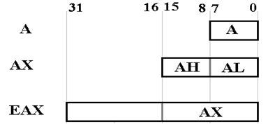
Structure of the
EAX register in the Intel 80386. There
is no name for the high–order
16 bits of EAX. The AX, AH, and
Backward Compatibility in the I/O Busses
Here is a figure
that shows how the PC bus grew from a 20–bit address through a 24–bit address
to a 32–bit address while retaining backward compatibility.
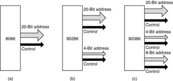
The requirement
is that I/O components (printers, disk drives, etc.) purchased for the Intel
8088
should be plug–compatible with both the Intel 80286 and Intel 80386. Those purchased for the
Intel 80286 should be plug–compatible with the Intel 80386. The basic idea is that one is more
likely to buy a new computer if the old peripheral devices can still be used.
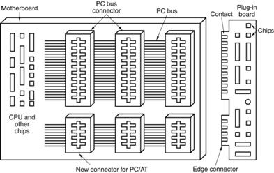
Here is a
picture of the PC/AT (Intel 80286) bus, showing how the original configuration
was
kept and augmented, rather than totally revised. Note that the top slots can be used by the
older
8088 cards, which do not have the “extra long” edge connectors. This cannot be used with cards
for the Intel 80386; that would be “forward compatibility”
The Intel 80386
was the first of the IA–32 series. In
you instructor’s opinion, it was the first
“real computer CPU” produced by Intel. The
reason for this opinion is that it was the first of the
series that had enough memory and a large enough address space to remove the
need for some
silly patches and kludges, such as extended and expanded memory.
1989 The Intel 80486 is introduced. It was aimed at higher performance. It was the first of
the Intel microprocessors to
contain one million transistors. As
noted above, later
variants of the 80486 were the
first to incorporate the floating point unit in the CPU core.
1992 Intel attempts to introduce the Intel
80586. Finding that it could not get a trademark
on
a number, Intel changed the
name to “Pentium”. The name “80586” was
used briefly as
a generic name for the Pentium
and its clones by manufacturers such as AMD.
1995 The Pentium Pro, a higher performance
variant of the Pentium was introduced.
It had
four new instructions, three
to support multiprocessing.
1997 The MMX (Multimedia Extensions) set of 57
instructions was added to both the Pentium
and the Pentium Pro. These facilitate graphical and other
multimedia computations.
1999 The Pentium III was introduced, with the SSE
(Streaming SIMD Extensions) instruction
set. This involved the addition of eight 128–bit
registers, each of which could hold four
independent 32–bit floating
point numbers. Thus four floating point
computations could
be performed in parallel.
2001 The Pentium 4 was shipped, with another 144
instructions, called SSE2.
2003 AMD, a producer of Pentium clones, announced
its AMD64 architecture to expand the
address space to 64 bits. All integer registers are widened to 64
bits. New execution
modes were added to allow
execution of 32–bit code written for earlier models.
2004 Intel adopts the AMD64 memory model,
relabeling it EM64T (Extended Memory 64
Technology).
Most of the
IA–32 improvements since this time have focused on providing graphical services
to
the game playing community. Your
instructor is grateful to the gamers; they have turned
high–end graphical coprocessors into commodity items. One can get very good graphics card
really cheap. Consider the NVIDIA
GeForce 8600 graphics processor with 512 MB of 400 MHz
graphics memory (DDR transferring 32 bytes per clock cycle), a 675 MHz graphics
processor, supporting 2048 by 1536 resolution.
It costs $210 bundled with software.
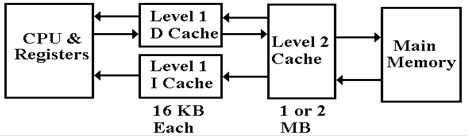
The Trace Cache
All
implementations of the Pentium architecture include at least two levels of
cache memory.
While we plan to discuss this topic in some detail later in this text, we must
bring it up now in
order to focus on a development in the architecture that began with the Pentium
III in 1999.
The earlier
Pentium designs called for a two–level cache, with a split L1 cache. There was a
16 KB L1 instruction cache and a 16 KB L1 data cache. Having the split L1 cache allowed the
CPU to fetch an instruction and access data in the same clock pulse. (Memory can do only one
thing at a time, but two independent memories can do a total of two things at a
time.) Here is a
figure showing a typical setup. Note
that the CPU does not write to the Instruction Cache.
By the time that
the Pentium III was introduced, Intel was having increasing difficulty in
obtaining fast execution of its increasingly complex machine language
instructions. The
solution was to include a step that converted each of the complex instructions
into a sequence
of simpler instructions, called micro–operations
in Intel terminology. These simpler
operations seem to be designed following the RISC (Reduced Instruction Set
Computer)
approach. Because these micro–operations
are simpler than the original, the CPU control unit
to interpret them can be hardwired, simpler, and faster.
By the time the
Pentium 4 was introduced, this new design approach had lead to the replacement
of the 16 KB Level–1 Instruction Cache with the ETC (Execution Trace Cache). Unlike the
Instruction cache, which holds the original Pentium machine language instructions,
the ETC
holds the micro–operations that implement these instructions.
Sixteen–bit Addressing
The Intel 8086
and later use a segmented address system in order to generate addresses from
16–bit registers. Each of the main
address registers was paired with an offset.
The IP
(Instruction Pointer) register is paired with the CS (Code Segment) register.
Each of the IP and CS is a 16–bit register in the earlier designs.
NOTE: The Intel terminology is far
superior to the standard name, the PC (Program
Counter), which is so named because it does not count anything.
The SP (Stack Pointer) register is paired
with the SS (Stack Segment)
register.
The Intel 8086
used the segment:offset approach to generating a 20–bit address.
The steps are as follows.
1. The
16–bit value in the segment register is treated as a 20–bit number
with four leading binary
zeroes. This is one hexadecimal 0.
2. This
20 bit value is left shifted by four, shifting out the high order four 0 bits
and shifting
in four low order 0 bits. This is equivalent to adding one hexadecimal
0.
3. The
16–bit offset is expanded to a 20–bit number with four leading 0’s
and added to the shifted
segment value. The result is a 20–bit
address.
Example: CS = 0x1234 and IP = 0x2004.
CS with 4 trailing
0’s: 0001 0010 0011
0100 0000 or 0x12340
IP with 4 leading
0’s: 0000 0010 0000
0000 0100 or 0x02004
Effective address: 0001 0100 0011
0100 0100 or 0x13344
Thirty–Two Bit Addressing
All computers in
the IA–32 series must support the segment:offset method of addressing in
order to run legacy code. This is “backwards compatibility”.
The native
addressing mode in the IA–32 series is called a “flat address space”. The 16–bit IP
(Instruction Pointer) is now the lower order 16 bits of the EIP (Extended
Instruction Pointer),
which can be used without a segment. The
16–bit SP (Stack Pointer) is now the lower order 16
bits of the ESP (Extended Stack Pointer), which also can be used without a
segment.
This diversity
of addressing modes has given rise to a variety of “memory models” based on
the addressing needed for code and data.
Memory Models: These
are conventional assembly language models based on the
size
of the code and the size of the data.
Code Size Data Size Model
to Use
Under 64 KB Under 64 KB Small
or Tiny
Over 64KB Under 64 KB Medium
Under 64 KB Over 64 KB Compact
Over 64 KB Over 64 KB Large
The smaller
memory models give rise to code that is more compact and efficient.
The IA–32 Register Set
The IA–32
register set contains eight 32–bit registers that might be called “general
purpose”,
though they retain some special functions.
These registers are: EAX, EBX, ECX, EDX, ESP,
EBP, ESI, and EDI. These are the 32–bit
extensions of the 16–bit registers AX, BX, CD, DX,
SP, BP, SI, and DI.
The 16–bit
segment registers (CS, DS, SS, ES, FS and GS) appear to be retained only for
compatibility with earlier code.
In the original
Intel 8086 design, the AX register was considered as a single accumulator,
with the other registers assigned supporting roles. It is likely that most IA–32 code maintains
this distinction, though it is not required.
The IA–64 Architecture
The IA–64
architecture is a design that evolved from the Pentium 4 implementation of the
IA–32
architecture. The basic issues involve
efficient handling of the complex instruction set that has
evolved over the 35 year evolution of the basic design. The IA–64 architecture is the outcome of
collaboration between Intel and the Hewlett–Packard Corporation. In some sense, it is an
outgrowth of the Pentium 4.
The IA–64
architecture has many features similar to RISC, but with one major exception:
it expects a sophisticated compiler to issue machine language that can be
exploited by the
superscalar architecture. (Again, we
shall discuss this in the future.) The
current
implementations of the IA–64 are called the “Itanium” and “Itanium 2”. One
wonders if the
name is based on that of the element Titanium.
In any case, the geeks soon started to call the
design the “Itanic”, after the ship “Titanic”, which
sank in 1912. The Itanium was released
in
June 2001: the Itanium 2 in 2002.
Here are some of
the features of the IA–64 design.
1. The
IA–64 has 128 64–bit integer registers and 128 82–bit floating–point registers.
2. The
IA–64 translates the binary machine language into 128–bit instruction words
that represent up to three
assembly language instructions that can be executed
during one clock pulse. A sophisticated compile emits these 128–bit
instructions
and is responsible for
handling data and control dependencies.
More on this later.
3. The
design might be called “VLIW” (Very Long Instruction Word) except that
Intel seems to prefer “EPIC”
(Explicitly Parallel Instruction Computing).
4. The
design allows for predicated execution, which is a technique that can eliminate
branching by making the
execution of the instruction dependent on the predicate.
There are sixty–four 1–bit
predicate registers, numbered 0 through 63.
With one
exception, each can hold a 0
(false) or a 1 (true). Predicate
register pr0 is fixed at
1 (true). Any instruction predicated on pr0 will always execute.
For
a full appreciation of predication, one would have to understand the design of
a pipelined
CPU, especially the handling of control hazards. This is a topic for a graduate course. Here
we shall just give a simple code example to show how it works. Consider the statement:
if (p) then S1 else S2 ; where S1 and
S2 are statements in the high level language.
Under
normal compilation, this would be converted to a statement to test the predicate (Boolean
expression that can be either true or false), execute a conditional branch
around statement S1,
and follow S1 by an unconditional branch around S2. In predication, the compilation is simpler,
and equivalent to the following two statements.
(p) S1 ; // Do this if the predicate is true.
(~p) S2 ; // Do this if the predicate
is false.
The
execution of this pair of statements is done together, in parallel with
evaluation of the
predicate. Depending on the value of the
predicate, the effect of one of the instructions is
committed to memory, and the results of the other statement are discarded.
One
of the goals of advanced architectures is the execution of more than one
instruction at a
time. This approach, called “superscalar”, must detect which
operations can be executed in
parallel, and which have data dependencies that force sequential execution.
In
the design of pipelined control units, these data dependencies are called “data hazards”.
Here is an example of a pair of instructions that present a data hazard.
x = y – z ;
w = u + x ;
Note
that these two instructions cannot be executed in parallel, while the next pair
can be
so executed. In the first set, the first
instruction changes the value of x. Parallel execution
would use the old value of x and hence yield
an incorrect result.
x = y – z ;
w = u + z ; // This pair can be executed in parallel.
Early
designs, dating back to the CDC-6600, used a hardware mechanism to detect which
instructions could be executed in parallel.
The difficulty with this approach is the increasing
complexity of such a control unit, leading to slower execution. The IA–64 strategy is called
“explicit parallelism”, in which the
compiler statically schedules instructions for parallel
execution at compile time, rather than the control unit do so dynamically at
run time.
IA–64
calls for the compiler to emit 128–bit bundles,
each containing three instructions, and
a template that defines which of the parallel execution units are to be
used. Each of the three
instructions in a bundle is called a syllable. Here is the structure of a bundle.
|
Instruction
Slot 2 |
Instruction
Slot 1 |
Instruction
Slot 0 |
Template |
|
41 bits |
41 bits |
41 bits |
5 bits |
Here is the instruction of a
syllable, fit into an instruction slot.
|
Major
Opcode |
More
of the instruction |
Predicate
Register |
|
4 bits |
31 bits |
6 bits |
Multicore Processors
The
CPU design problem, called the “power
wall” was discussed in chapter 1 of this text. The
commonly accepted solution to this problem, in which designers try to get more
performance
from a CPU without overheating it, is called a multicore CPU. This is
basically a misnomer,
because each core in a multicore CPU is an independent CPU. Thus a quad–core Pentium chip
actually contains four CPUs. Examples of
this strategy include the Intel iCore3, iCore5, and
iCore7 (sometimes called “Core i3”, “Core i5”, and “Core i7”) designs. The i3 is the entry level
processor, with two cores. The i5 is a
mid–range processor with 2 to 4 cores.
The i7 is
considered to be the high–end processor, with 2 to 6 cores.
Motherboards and
slots
Along
with the evolution of the CPU chips, we see an evolution of the support
hardware.
Here we study the hardware used to integrate the CPU into the system as a
whole.
Sockets
A CPU socket or CPU
slot is a mechanical component that provides mechanical and electrical
connections between a device (usually a microprocessor) and a printed circuit
board (PCB), or
motherboard. This allows the CPU to be replaced without risking the damage
typically
introduced when using soldering tools [R016].
Common sockets utilize retention clips that are
designed to apply a constant force, which must be overcome when a device is
inserted. For chips
that sport a high number of pinouts, either
zero-insertion force (ZIF) sockets or land grid array
(LGA) sockets are used instead. These designs apply a compression force once
either a handle
(for ZIF type) or a surface plate (LGA type) is put into place. This provides
superior mechanical
retention while avoiding the added risk of bending pins when inserting the chip
into the socket.
CPU sockets are used in desktop
computers (laptops typically use surface mount CPUs) because
they allow easy swapping of components, they are also used for prototyping new
circuits.
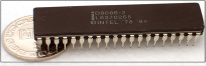
The earliest sockets were quite
simple, in fact they were DIP (Dual In–line Pin) devices. A
typical CPU for such a slot might be an Intel 4004 or an Intel 8086 (with
different pin count).
Here is a picture of the Intel 8086, showing one of the two rows of pins.
The complexity of the IA–32
series processors grew as the series evolved, and the number
of pin–outs required grew with it. By
the time of the Intel 80486, a DIP arrangement was
impossible. Here is a picture of the Intel
80486DX2.
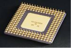 The Intel 80486 had 196 pins arranged
as a hollow
The Intel 80486 had 196 pins arranged
as a hollow
rectangle. It should be obvious that it
required more
than a DIP socket.
The sockets for the late Intel
80x86 series and the early
Pentium series came in a number of sizes in order to
accommodate the number of pins on the chip.
Here is a table of some of the
early sockets used for the IA–32 series.
|
Socket |
Year
introduced |
CPU
families |
Package |
Pin
count |
Bus
speed |
|
DIP |
1970s |
Intel 8086, Intel 8088 |
DIP |
40 |
5/10 MHz |
|
Socket
1 |
1989 |
Intel 80486 |
PGA |
169 |
16–50 MHz |
|
Socket
2 |
? |
Intel 80486 |
PGA |
238 |
16–50 MHz |
|
Socket
3 |
1991 |
Intel 80486 |
PGA |
237 |
16–50 MHz |
|
Socket
4 |
? |
Intel Pentium |
PGA |
273 |
60–66 MHz |
|
Socket
5 |
? |
Intel Pentium, AMD K5 |
PGA |
320 |
50–66 MHz |
|
Socket
6 |
? |
Intel 80486 |
PGA |
235 |
? |
|
Socket
7 |
1994 |
Intel Pentium, Intel Pentium MMX, AMD K6 |
PGA |
321 |
50–66 MHz |
|
Socket
8 |
1995 |
Intel Pentium Pro |
PGA |
387 |
60–66 MHz |
Slots
With the introduction of the
Pentium II CPU, the transition from socket to slot had become
necessary. With the Pentium Pro, Intel had combined processor and cache dies in
the same
package, connected by a full-speed bus, resulting in significant performance
benefits.
Unfortunately, this method required that the two components be bonded together
early in the
production process, before testing was possible. As a result, a single, tiny
flaw in either die made
it necessary to discard the entire assembly, causing low production yield and
high cost.
Intel subsequently designed a
circuit board where the CPU and cache remained closely
integrated, but were mounted on a printed circuit board, called a Single-Edged
Contact Cartridge
(SECC). The CPU and cache could be tested separately, before final assembly
into a package,
reducing cost and making the CPU more attractive to markets other than that of
high-end servers.
These cards could also be easily plugged into a Slot 1, thereby eliminating the
chance for pins of
a typical CPU to be bent or broken when installing in a socket.
Slot 1 refers to the
physical and electrical specification for the connector used by some of Intel's
microprocessors, including the Pentium Pro, Celeron, Pentium II and the Pentium
III. Both
single and dual processor configurations were implemented. Slot 1 (also Slot1 or SC242) is a
Slot-type
connector with 242 contacts. This connector was designed for Pentium II family
of
processors,
and later used for Celeron budget line of processors. Pentium III was the last
microprocessor
family that used the Slot 1. For its next generation of Pentium processors -
Pentium
4, Intel completely abandoned the Slot1 architecture. The fastest processor
that can be
used
in the Slot 1 motherboards is the Pentium III 1133 MHz with 133 MHz FSB [R012].
The
picture
on the left shows a typical slot 1 connector mounted on a motherboard. The picture at
right
shows a CPU mounted in the slot, along with its rather large cooling fans.
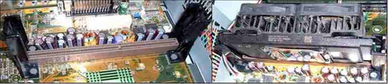
Slot
1 connector is 5.23" long (13.29 cm). Besides the actual connector, the
Slot 1 also includes
SEC
cartridge retention mechanism required to support a processor in SEC cartridge
and a
heatsink.
Maximum supported weight of the processor with the heatsink is 400 grams.
Slot 2 refers to the
physical and electrical specification for the 330-lead Single Edge Contact
Cartridge (or edge-connector) used by some of Intel's Pentium II Xeon
and certain models of the Pentium III Xeon.
When first introduced, Slot 1 Pentium IIs were intended to replace the
Pentium and Pentium Pro processors in the home, desktop, and low-end SMP
markets. The
Pentium II Xeon, which was aimed at multiprocessor workstations and
servers, was largely
similar to the later Pentium IIs, being based on the same P6 Deschutes
core, aside from a wider
choice of L2 cache ranging from 512 to 2048 KB and a full-speed off-die
L2 cache (the Pentium
2 used cheaper 3rd party SRAM chips, running at 50% of CPU speed, to
reduce cost).
Because the design of the 242-lead Slot 1 connector did
not support the full-speed L2 cache of
the Xeon, an extended 330-lead connector was developed. This new
connector, dubbed 'Slot 2',
was used for Pentium 2 Xeons and the first two Pentium III Xeon cores,
codenamed 'Tanner' and
'Cascades'. Slot 2 was finally replaced with the Socket 370 with the Pentium
III Tualatin; some
of the Tualatin Pentium IIIs were packaged as 'Pentium III' and some as
'Xeon', despite the fact
they were identical [R014].
Socket 370 (also known as the
PGA370 socket) is a common format of CPU socket first used by
Intel for Pentium III and Celeron processors to replace the older Slot
1 CPU interface on
personal computers. The "370" refers to the number of pin
holes in the socket for CPU pins.
Modern Socket 370 fittings are usually found on Mini-ITX motherboards
and embedded systems
[R015]. Here is a picture of the
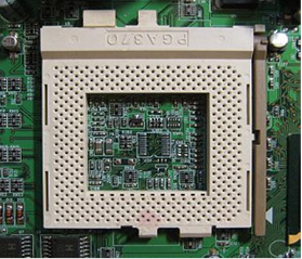
PGA370 socket.
 The socket is a ZIF (Zero Insertion Force) type,
designed for easy insertion. As
noted, it has 370
pin connectors.
The
dimensions are 1.95 inches by 1.95 inches, or
approximately 5 centimeters on a side.
This
was designed to work with a Front Side Bus
operating
at 66, 100, or 133 MHz. The design
voltage
range is 1.05 to 2.10 volts.
The
mass of the Socket 370 CPU cooler should not
exceed
180 grams (a weight of about 6.3 ounces)
or
damage to the die may occur.
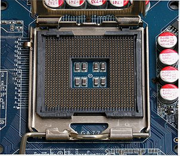
The LGA 775, also known as Socket T, is one of the latest and
largest Intel CPU sockets . LGA
stands for land grid array.
Unlike earlier common CPU sockets, such as its predecessor Socket
478, the LGA 775 has no socket holes; instead, it has 775 protruding
pins which touch contact
points on the underside of the processor (CPU).
The Prescott and Cedar Mill Pentium 4 cores, as well as
the Smithfield and Presler Pentium D
cores, used the LGA 775 socket. In July 2006, Intel released the desktop
version of the Core 2
Duo (codenamed Conroe), which also uses this socket, as does the
subsequent Core 2 Quad. Intel
changed from Socket 478 to LGA 775 because the new pin type offers
better power distribution
to the processor, allowing the front side bus to be raised to 1600 MT/s.
The 'T' in Socket T was
derived from the now cancelled Tejas core, which was to replace the
Prescott core. Another
advantage for Intel with this newer architecture is that it is now the
motherboard which has the
pins, rather than the CPU, transferring the risk of pins being bent from
the CPU to the
motherboard.
The CPU is pressed into place by a "load plate",
rather than human fingers directly. The
installing technician lifts the hinged "weld plate", inserts
the processor, closes the load plate
over the top of the processor, and pushes down a locking lever. The
pressure of the locking
lever on the load plate clamps the processor's 775 copper contact points
firmly down onto the
motherboard's 775 pins, ensuring a good connection. The load plate only
covers the edges of
the top surface of the CPU (processor heatspreader). The center is free
to make contact with the
cooling device placed on top of the CPU.
An examination of the relevant Intel data sheets shows
that LGA 775 which is used for consumer
level desktops and LGA 771 used for (Xeon based) workstation and server
class computers
appear to differ only in the placement of the indexing notches and the
swap of two address pins.
Many pins devoted to functions such as interfacing multiple CPUs are not
clearly defined in the
LGA 775 specifications, but from the information available appear to be
consistent with those of
LGA 771. Considering that LGA 775 predated LGA 771 by nearly a year and
a half, it would
seem that LGA 771 was adapted from LGA 775 rather than the other way
around.
The socket has been superseded by the LGA 1156 (Socket H)
and LGA 1366 (Socket B) sockets.
Here
is a picture from [R017] of the LGA 775 mounted on some sort of motherboard.