There is one
real–mode data structure that requires discussion, as it will lead to a more
general data structure used in protected mode.
This is the IVT (Interrupt Vector Table),
which is used to activate software associated with a specific I/O device. We shall discuss
I/O management, including I/O interrupts and I/O vectors in chapter 9 of this
text. Here is
the brief description of an input I/O operation to show the significance of the
IVT.
1. An
I/O device signals the CPU that it is ready to transfer data by asserting a
signal called an “interrupt”. This is asserted low.
2. When
the CPU is ready to handle the transfer, it sends out a signal, called an
“acknowledge” to initiate the I/O process itself.
3. As
a first step to the I/O process, the device that asserted the interrupt
identifies
itself to the CPU. It does this by sending a vector, which is merely an address to
select an entry in the
IVT. The IVT should be considered as an
array of entries,
each of which contains the
address of the program to handle a specific I/O device.
4. The
ISR (Interrupt Service Routine) appropriate for the device
begins to execute.
There
is more to the story than this, but we have hit the essential idea of a single
IVT to
manage the input and output for all executing programs.
Protected mode is the native state of the
Pentium processor, in which all instructions and
features are available. Programs are
given separate memory areas called segments,
and the
processor uses the segment registers and associated other registers to manage
access to memory,
so that no program can reference memory outside its assigned area. The operating system is
thus protected from intrusion by user programs.
The operating system operates in a privileged
state in which it can change the segment registers in order to access any area
of memory.
Virtual 8086 mode is a sub–mode of protected
mode. In this mode, many of the
protection
features of protected mode are active.
The processor can execute real–mode software in a safe
multitasking environment. If a virtual
8086 mode process crashes or attempts to access memory
in areas reserved for other processes or the operating system, it can be
terminated without
adversely affecting any other process.
In protected
mode, and its sub–mode virtual 8086 mode, each process is assigned a separate
session, which allows for proper
management of its resources. Part of
that management involves
creation of a separate IVT for that session, allowing the Pentium to allocate
different I/O services
to separate sessions. More importantly
it provides protection against software crashes.
Windows XP can
manage multiple separate virtual 8086 sessions at the same time, possibly in
parallel with execution of programs in protected mode. This idea has been extended successfully
to that of a virtual machine, in
which a number of programs can execute on a given machine
without affecting other programs in any way.
The large IBM mainframes, including the
z/9 and z/10, call this idea an LPAR
(Logical Partition).
One key logical
component of the virtual machine idea has yet to be discussed; this is called
virtual memory. This will be discussed fully in chapter 12 of
this textbook. There is one
important point that can be restated even at this early stage. The program generates addresses
that are modified by the operating system into actual addresses into physical
memory. As a
result, the operating system controls access to real physical memory and can
use that control to
enhance security.
In protected
mode, as well as in its sub–mode virtual 8086, addresses to physical memory are
generated in a number of steps. Three
terms related to this process are worth mention: the
effective address, linear address, and physical address. With the exception of the term
“physical address”, which references
the actual address in the computer memory, the terms
are somewhat contrived. In the IA–32
designs, the effective address is
the address generated by
the program before modification by the memory management unit. The rules for generation of
this address are specified by the syntax of the assembly language.
The effective
address is passed to the memory management unit, first to the segmentation
unit,
which accesses the segment registers to create the linear address and then accesses a number of
other MMU (Memory Management Unit) registers to determine the
validity of the address value
and the validity of the access: read, write, execute, etc. The translation from linear address to
physical address is controlled by the virtual memory system, the topic of a
later chapter.
Cache Memory
Here is another
topic that we continue to mention in passing with a promise to discuss it more
fully at a later time. For the moment,
we shall describe the advantages of such a system, and
again postpone a full discussion for another chapter.
Each Pentium
product is packaged with a cache memory system designed to optimize memory
access in a system that is referencing both data memory and instruction memory
at the same
time. We should note that it is the
general practice to keep both data and executable instructions
in the same main memory, and differentiate the two only in the cache. This is one example of
the common use of cache: cause the memory system to act as if it has a certain
desirable attribute
without having to alter the large main memory to actually have that attribute.
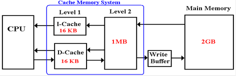
At this time,
let’s state a few facts. Because it is
smaller, the Level 1 cache (L1 cache) is faster
than the L2 cache. Because it is smaller
than main memory, the L2 cache is faster than the main
memory. This multilevel cache applies
the same trick twice. In the above
example, the 32 KB
L1 cache combined with the 1 MB L2 cache acts as if it were a single cache
memory with an
access time only slightly slower than the actual L1 cache. Then the combination of cache
memory and the main memory acts as if it were a single large memory (2 GB) with
an access
time only slightly slower than the cache memory. Now we have a memory that functionally is
both large and fast, while no single element actually has both attributes.
Recent main
memory designs have added a write buffer, allowing for short bursts of memory
writes at a rate much higher than the main memory can sustain. Suppose that the main memory
has a cycle time of 80 nanoseconds, requiring a 80 nanosecond time interval
between two
independent writes to memory. A fast
write buffer might be able to accept eight memory writes
in that time span, sending each to main memory at a slower rate.
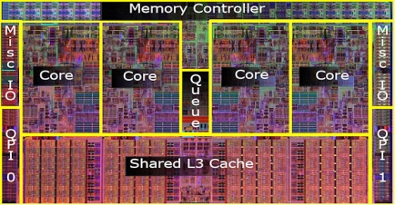
We mention in
passing that some multi–core Pentium designs have three levels of cache
memory. Here is a picture of the Intel
Core i7 die. This CPU has four cores, each
with its
L1 and L2 caches. In addition, there is
a Level 3 cache that is shared by the four cores. This
design illustrates two realities of CPU design in regards to cache memory.
1. The
placement of cache memory on the CPU chip significantly increases execution
speed, as on –chip accesses
are faster than accesses to another chip.
2. Better
power management, due to the fact that memory uses less power per unit area
than does the CPU logic.
Register Sets
Almost all
modern computers divide storage devices into three classes: registers, memory,
and
external storage (such as disks and magnetic tape). In earlier times, the register set (also
called
the register file) was distinctly associated with the CPU, while main memory
was obviously
separate from the CPU. Now that designs
have on–chip cache memory, the distinction between
register memory and other memory is purely logical. We shall see that difference when we study
a few fragments of IA–32 assembly language.
One of the first
steps in designing a CPU is the determination of the number and naming of the
registers to be associated with the CPU.
There are many general approaches, and then there is
the approach seen on the Pentium. The
design used in all IA–32 and some IA–64 designs is a
reflection of the original Intel 8080 register set.
Register set of
the Intel 8080 and 8086
The original
Intel 8080 and Intel 8086 designs date from a time when single accumulator
machines were still common. As mentioned
in a previous chapter, it is quite possible to design
a CPU with only one general–purpose register; this is called the accumulator. The provision of
seven general–purpose registers in the Intel 8080 design was a step up from
existing practice.
We have already
discussed the evolution of the register set design in the evolution of the
IA–32
line. The Intel 8080 had 8–bit
registers; the Intel 8086, 80186, and 80286 each has 16–bit
registers, and the IA–32 line (beginning with the Intel 80386) all have 32–bit
registers. The
Intel 8080 set the trend; newer models might have additional registers, but
each one had to have
the original register set in some fashion.
Register set of
the Intel 80386
The Intel 80386
was the first member of the IA–32 design line.
It is a convenient example for
purposes of discussion. In fact, it is
common practice for introductory courses in Pentium
assembly language to focus almost exclusively on the Intel 80386 Instruction
Set Architecture
(register set and assembly language instructions), and to treat the full
Pentium ISA as an
extension. Here is a figure showing the
Intel 80386 register set.
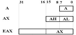
EAX:
This is the general–purpose register used for arithmetic and logical
operations. Recall
from the previous chapter that parts of this register can be separately
accessed. This division is
seen also in the EBX, ECX, and EDX registers; the code can reference BX, BH,
CX, CL, etc.
This register
has an implied role in both multiplication and division. In addition, the A register
(AL in the Intel 80386 usage) is involved in all data transfers to and from the
I/O ports.
Here are some
examples of IA–32 assembly language involving the EAX register. Note that
the assembly language syntax denotes hexadecimal numbers by appending an “H”.
MOV EAX, 1234H
; Set the value of EAX to hexadecimal 1234
; The format is
destination, source.
CMP AL, ‘Q’
; Compare the value in AL (the low order 8
; bits of EAX to 81,
the ASCII code for ‘Q’
MOV ZZ, EAX
; Copy the value in EAX to memory location ZZ
DIV DX
; Divide the 32-bit value in EAX by the
; 16-bit value in DX.
Here is an
example showing the use of the AX register (AH and AL) in character input.
MOV AH, 1 ; Set AH to 1 to indicate the desired I/O
; function – read a
character from standard input.
INT 21H ; Software interrupt to invoke an
Operating System
; function, here the value
21H (33 in decimal)
; indicates a standard I/O
call.
MOV XX, AL ; On return from the function call, register
AL
; contains the ASCII code
for a single character.
; Store this in memory
location XX.
EBX:
This can be used as a general–purpose register, but was originally
designed to be
the base register, holding the address of the base of a data structure. The easiest example of
such a data structure is a singly dimensioned array.
LEA EBX, ARR ; The LEA instruction loads the address
; associated with a label
and not the value
; stored at that
location.
MOV AX, [EBX] ; Using
EBX as a memory pointer, get the 16-bit
; value at that address
and load it into AX.
ADD EAX, EBX ; Add the 32-bit value in EBX to that in EAX.
ECX:
This can be used as a general–purpose register, but it is often used in
its special role as
a counter register for loops or bit shifting operations. This code fragment illustrates its use.
MOV EAX, 0 ; Clear the accumulator EAX
MOV ECX, 100 ; Set the count to 100 for 100 repetitions
TOP: ADD EAX, ECX ; Add
the count value to EAX
LOOP TOP ; Decrement ECX, test for zero, and jump
; back to TOP if
non-zero.
At the end of
this loop, EAX contains the value 5,050.
EDX:
This can be used as a general–purpose register, but it can also support
input and output
data transfers. It also plays a special
part in executing integer multiplication and division. In
general, the product of two 8–bit integers is a 16–bit integer, the product of
two 16–bit integers
is a 32–bit integer, and the product of two 32–bit integers is a 64–bit
integer. Remember that
register AL is the 8 low–order bits of EAX, and AX is the 16 low–order bits.
One item that is
important to note is that the EAX register, or whatever part is used in the MUL
operation, is implicitly a part of the operation, without being called out
explicitly.
MOV AL, 5H ;
Move decimal 5 to AL
MOV BL, 10H ; Decimal 16 to BL
MUL BL ; AX gets the 16–bit number 0050H (80
decimal)
; The instruction says
multiply the value in
; AL by that in BL and
put the product in AX.
; Only BL is explicitly
mentioned.
The 16–bit
multiplications use AX as a 16–bit register.
For compatibility with the Intel 8086,
the full 32 bits of EAX are not used to hold the product. Rather the two 16–bit registers AX and
DX are viewed as forming a 32–bit pair and serve to store it. Again, note that the 16–bit version
of the MUL automatically takes AX as holding one of the integers to be
multiplied.
MOV AX, 6000H ;
MOV BX, 4000H ;
MUL BX ; DX:AX = 1800 0000H.
The 32–bit
implementation of multiplication uses EAX to hold one of the integers to be
multiplied and uses the register pair EDX:EAX to hold the product. Here is an example.
MOV EAX, 12345H
MOV EBX, 10000H
MUL EBX ; Form the product EAX times EBX
; EDX:EAX = 0000 0001
2345 0000H
Register DX can
also hold the 16–bit port number of an I/O port.
MOV DX, 0200H
IN
AL, DX ; Get a byte from the
port at address 200H.
The ESI and EDI registers are used as source and destination addresses for
string and array
operations. These are sometimes called “Extended Source Index” and “Extended Destination
Index”. They facilitate high–speed
memory transfers.
The EBP register is used to support the
call stack for high level language procedure calls. We
shall discuss this more in the next chapter, in which we discuss subroutines. Briefly put, it
functions much like a stack pointer, but does not point to the top of the
stack.
The next two registers,
EIP and ESP, are 32–bit versions of the older 16–bit counterparts. We
discuss these here, and then introduce the 16–bit variants by discussing
segments again.
The EIP is the 32–bit Instruction Pointer, so called because it points to the instruction
likely to
be executed next. Many other
architectures call this register by the more traditional, if less
appropriate, name “Program Counter”. Jump and branch instructions, unconditional
or
conditional (if the condition is true), achieve their affect by forcing a
target address into the EIP.
The ESP is the 32–bit Stack Pointer, used to hold the address of the top of the stack. This
register is not commonly accessed directly except as a part of a procedure
call. We must make
the point here that the stack is not always treated as an ADT (Abstract Data Type) with PUSH as
the only way to place an item on the stack.
We shall investigate direct manipulation of the ESP
in more detail when we discuss allocation of dynamic memory for local
variables.
The EFLAGS register holds a collection of
at most 32 Boolean flags with various meanings.
The flags are divided into two broad categories: control flags and status
flags. Control flags
can cause the CPU to break after every instruction (good for debugging),
interrupt execution on
detecting arithmetic overflow, enter protected mode, or enter virtual 8086
mode.
The status flags
reflect the state of the execution and include CF (the carry flag, indicating a
carry out of the last arithmetic operation), OF (the overflow flag, indicating
that the result is
too large or too small to be represented), SF (the sign flag, indicating that
the last result was
negative), ZF (the zero flag, indicating that the last result was zero), and
several more.
There are six
16–bit segment registers (CS, SS, DS, ES, FS, and GS), which are hold overs
from the 16–bit Intel 8086. As discussed
in the previous chapter, these are used to allow
generation of 20–bit addresses from 16–bit registers. The two standard register pairings are
CS:IP (Code Segment and Instruction Pointer) and SS:SP (Stack Segment and Stack
Pointer).
In the more modern Pentium usage, these segment registers are used in
combination with
descriptor registers to support memory management.
Register set of
the Pentium
In addition to
the above register set, the Pentium architecture calls for six 64–bit registers
to
support memory management (CSDCR, SSDCR, DSDCR, ESDCR, FSDCR, and GSDCR), the
TR (Task Register), the IDTR (Interrupt Descriptor Table Register), two
descriptor registers
(GDTR – Global Descriptor Task Register and LDTR – Local Descriptor Task
Register) and a
few more. Then there are the sixteen
specialized data registers (MM0 – MM7 for the multimedia
instructions, and FP0 – FP7 for floating point arithmetic). Newer versions of the architecture
almost certainly contain still more registers.
Especially in
the case of memory management, it is important to remember that the Operating
System functions by setting up and then using some fairly elaborate data
structures. Each of
these structures has a base address stored in one of these registers for fast
access.
Addressing Modes
We now discuss
some of the addressing modes used in the Pentium architecture. We shall use
two–argument instructions to illustrate this, as that is easier. The simplest mode is also the
fastest to execute. This is the data register direct mode. Here is an example.
MOV EAX, EBX ; Copy the value from EBX into EAX
; The value in EBX is
not changed.
Immediate Mode
In this mode,
one of the arguments is the value to be used.
Here are some examples, a few
of which are not valid.
MOV EBX, 1234H ; EBX gets the value 01234H.
MOV 123H, EBX ; NOT VALID.
The destination of any
; move must be a
memory location.
MOV AL, 1234H ; NOT VALID.
Only one byte can be moved
; into an 8-bit
register. This is 2 bytes.
Memory Direct Mode
In this mode,
one of the arguments is a memory location.
Here are some examples.
MOV ECX, [1234H] ; Move the value at address 1234H to ECX.
; Not the same as the
above example.
MOV EDX, WORD1 ; Move the contents of address WORD1 to EDX
MOV WORD2, EDX ; Move the contents of the 32–bit register
; EDX to memory
location WORD2.
MOV X, Y ; NOT VALID. Memory to memory moves are
; not allowed in this
architecture.
Address Register Direct
Here, the
address associated with a label is loaded into a register. Here are two examples,
one of which is memory direct and one of which is address register direct.
LEA EBX, VAR1
; Load the address associated with VAR1
; into register
EBX.
; This is address
register direct.
MOV EBX, VAR1
; Load the value at address VAR1 into EBX.
; This is memory
direct addressing.
Register Indirect.
Here the register
contains the address of the argument.
Here are some examples.
MOV EAX, [EBX] ; EBX contains the address of a value
; to be moved to
EAX.
Note that the
following two code fragments do the same thing to EAX. Only the first
fragment changes the value in EBX.
LEA EBX, VAR1 ; Load the address VAR1 into EBX
MOV EAX, [EBX] ; Load the value at that address into EAX
MOV EAX, VAR1 ; Load the value at address VAR1 into EAX
Direct Offset Addressing
Suppose an array
of 16–bit entries at address AR16. We may
employ direct offset in two ways
to access members of the array. Here are
a number of examples.
MOV CX,AR16+2 ; Load the 16–bit value at address
; AR16 + 2 into
CX. For a zero-based
; array, this might
be AR16[1].
MOV CX,AR16[2] ; Does the same thing. Computes the
; address (AR16 +
2).
Base Index Addressing
This mode
combines a base register with an index register to form an address.
MOV EAX, [EBP+ESI] ;
Add the contents of ESI to that of EBP
; to form the
source address. Move the
; 32–bit value at
that address to EAX.
Index Register with Displacement
There are two
equivalent versions of this, due to the way the assembler interprets the
second way. Each uses an address, here TABLE,
as a base address.
MOV EAX,
[TABLE+EBP+ESI] ; Add the contents of ESI to that
; of EBP to
form an offset, then add
; that to the
address associated
; with the
label TABLE to get the
; address of
the source.
MOV EAX TABLE[ESI] ; Interpreted as the same as above.