An Extended (Silly) Example of I/O Strategies
There are
four major strategies that can be applied to management of the I/O process:
Program-Controlled, and
Interrupt-Driven, and
Direct Memory Access, and
I/O Channel.
We try to
clarify the difference between these strategies by the example of having a
party in
one’s house to which guests are invited.
The issue here is balancing work done in the house to
prepare it for the party with the tasks of waiting at the front door to admit
the guests.
Program-Controlled
The analogy for
program-controlled I/O would be for the host to remain at the door, constantly
looking out, and
admitting guests as each one arrives.
The host would be at the door constantly
until the proper
number of guests arrived, at which time he or she could continue preparations
for
the party. While standing at the door, the host could do
no other productive work. Most of us
would consider that
a waste of time.
Interrupt-Driven
Many of us have
solved this problem by use of an interrupt mechanism called a doorbell. When
the doorbell rings,
the host suspends the current task and answers the door. Having admitted the
guest, the host can
then return to preparations for the party.
Note that this example contains, by
implication, several
issues associated with interrupt handling.
The first issue is priority. If the host
is in the process of putting out a fire in the kitchen, he or
she may not answer
the door until the fire is suppressed. A
related issue is necessary completion.
If the host has just
taken a cake out of the oven, he or she will not drop the cake on the floor to
answer the door, but
will first put the cake down on a safe place and then proceed to the door. In
this scenario, the
host’s time is spent more efficiently as he or she spends little time actually
attending the door
and can spend most of the time in productive work on the party.
Direct Memory Access
In this case, the
host unlocks the door and places a note on it indicating that the guests should
just open the door
and come in. The host places a number of
tickets at the door, one for each
guest expected, with
a note that the guest taking the last ticket should so inform the host. When
the guest taking the
last ticket has arrived, the host is notified and locks the door. In this
example the host’s
work is minimized by removing the requirement to go to the door for each
arrival of a
guest. There are only two trips to the
door, one at the beginning to set up for the
arrival of guests
and one at the end to close the door.
I/O Channel
The host hires a
butler to attend the door and lets the butler decide the best way to do
it. The
butler is expected
to announce when all the guests have arrived.
Note that the I/O channel is not really a distinct strategy. Within the context of our silly
example, we note that the butler will use one of the above three strategies to
admit guests. The
point of the strategy in this context is that the host is relieved of the
duties. In the real world
of computer I/O, the central processor is relieved of most I/O management
duties.
I/O Device Registers
From the viewpoint of the CPU, each I/O device is nothing more than a
set of registers. An
Input device is characterized by its input Data register from which the CPU
reads data. An
Output device is likewise characterized by its data register.
While the
I/O can be based on explicit knowledge of device timings, the more common
methods involve use of the registers to assert and test specific signals. Registers generally
fall into three classes, though simpler I/O devices may have a single register
with both
control bits (write only) and status bits (read only).
The
contents of the status and control registers are generally treated as a
collection of
individual bits. Upon occasion, each
register can be treated as if it were holding a signed
two’s–complement integer. In this case,
the sign bit may be set to indicate an error.
Data used for data to be read from or
written to the I/O device
for input
devices this is a read-only register
for output
devices this register is usually nor read by the CPU
Status used to report the device status. If the sign bit is 1, there has been
a device error. The assignment of the sign bit as an overall
error bit (other
bits for specific errors) is for ease of programming, as a
status register
with the error bit set will be read as a negative number.
Control used to set options on the I/O device
Disk drives
have control registers to select cylinder, track, sector, etc.
Extra four registers per device simplifies
the address calculations.
In these
designs, we shall ignore the Extra register.
Two Examples to Define Some Issues
Before discussing the details of
hardware I/O devices, it will be helpful to give two examples
in a high–level language. Each of these
will illustrate issues in the interfacing of software and
hardware as a part of the I/O process.
In particular, these examples should lead to a deeper
appreciation of the decision to structure the I/O software as multiple layers.
The examples will focus on input
and output of simple integer values. To
simplify the
discussion slightly, it will be assumed that the value zero will not be entered
or output; all
values are strictly positive or negative. Two more assumptions are significant.
1. The integer values are stored in 16–bit two’s–complement form.
2. The digits are encoded as ASCII characters.
The
examples will use the decimal numbers 123 and –123 (the negative number).
The binary representation of these two are as follows:
The positive number 123 is
represented as 0000
0000 0111 1011
The negative number –123 is
represented as 1111 1111 1000 0101
Here are the ASCII codes for the decimal digits..
|
Character |
‘0’ |
‘1’ |
‘2’ |
‘3’ |
‘4’ |
‘5’ |
‘6’ |
‘7’ |
‘8’ |
‘9’ |
|
Hexadecimal value |
30 |
31 |
32 |
33 |
34 |
35 |
36 |
37 |
38 |
39 |
|
Decimal value |
48 |
49 |
50 |
51 |
52 |
53 |
54 |
55 |
56 |
57 |
The table
above quickly illustrates how to convert between ASCII codes for single
digits and their numeric value. The
following pseudocode will be suggestive; in any
modern high–level language the expressions must include explicit type casting.
ASCII_Code = Numeric_Value + 48
// Decimal
Numeric_Value = ASCII_Code – 48
As an
aside, we note that the conversions might have been accomplished using the bit
manipulations allowed by the Boolean operators AND, OR, and NOT. Here, we have
elected to use the arithmetic operators.
Consider
the positive integer 123. Here we must
make a distinction between the integer
value and its print representation. This is a distinction that is not normally
made, as it
has few practical implications. Within
the context of I/O hardware and software, it is a
distinction worth noting. When we read
the string “123”, we say that it is the integer.
However, it is a three digit string that represents the integer value.
In our
example using 16–bit two’s–complement internal representation, the integer
value
that is stored internally as 0000 0000 0111 1011 is converted
to the digits ‘1’, ‘2’, and ‘3’
used to build the string “123”. The
string is sent to the output device. For
input, the process is
reversed. The string “123” will be
broken into three digits, and the numeric value of each digit
determined so that the integer value can be computed.
Output of a Non–Zero Integer Value
Here is a
pseudocode description for the process, using the values 123 and –123 as
illustrations.
The output string is built right to left, with the sign character placed last.
Output 123 Output –123
Binary: 0000 0000 0111 1011 Binary: 1111 1111 1000 0101
This is
not negative, set Sign_Char = ‘ ’ This is negative, set Sign_Char = ‘–’
Value to convert is 123 Value
to convert is 123.
Divide 123
by 10 to get the remainder 3, with quotient 12.
Add 48
to the remainder to get the ASCII code for ‘3’.
Place
‘3’ in the string. “3”.
Divide 12 by
10 to get the remainder 2, with quotient 1.
Add 48
to get the code for ‘2’ and place in the string to get “23”.
Divide 1 by
10 to get the remainder 1, with quotient 0.
Add 48
to get the code for ‘1’ and place in the string to get “123”.
Stop as the quotient is 0.
Place the sign character to get “ 123”. Place the sign character to get “–123”.
Send the output string to the output device.
Input of a String Representing a Non–Zero
Integer Value
The input
string is scanned left to right. The
scan will detect either the sign ‘–’ or a digit.
The leftmost digit is assumed to begin the print representation of the absolute
value of the
integer. Admittedly, an
industrial–strength algorithm would do much more.
Input “123” Input “–123”
First
character found is a digit. First
character found is ‘–’.
The value is not negative. The
value is negative.
Set Is_Negative = False. Set Is_Negative
= True.
Scan
for next character. It is a digit.
Digit = ‘1’ Digit
= ‘1’
Set Number_Value = 0 to initialize the process.
Strip the
leftmost digit from the input string.
Digit = ‘1’.
Now
the input string is String = “23”.
Subtract 48
from the 49, the ASCII code for ‘1’ to get the value 1.
Digit_Value = 1
Set Number_Value = Number_Value · 10 +
Digit_Value
Number_Value = 1.
Strip the
leftmost digit from the input string.
Digit = ‘2’.
Now
the input string is String = “3”.
Subtract 48
from the 50, the ASCII code for ‘2’ to get the value 2.
Digit_Value = 2
Set Number_Value = Number_Value · 10 +
Digit_Value
Number_Value = 12.
Strip the
leftmost digit from the input string.
Digit = ‘3’.
Now
the input string is String = “” (the empty string).
Subtract 48
from the 51, the ASCII code for ‘3’ to get the value 3.
Digit_Value = 3
Set Number_Value = Number_Value · 10 +
Digit_Value
Number_Value = 123.
The input string is empty, so stop this process.
The value
is not negative. The
value is negative.
Take
the two’s complement.
Value
stored is 123 Value
stored is –123.
Binary: 0000
0000 0111 1011 Binary:
1111
1111 1000 0101
One
motivation for this tedious discussion is to point out part of the complexity
of the
process of integer value input and output.
It is one of the main advantages of a high–level
language and its run–time support system (RTS) that a programmer can ignore
these details
and focus on the solution to the problem at hand. One of the goals of this course is to focus
on these details, so that the student will gain an appreciation of the
underlying process.
Overview of the Output Process
We continue
the discussion of the processes associated with output of a representation of
an
integer value to an output device. The
purpose of this part of the discussion is to show that
the process naturally suggests layers of software, also called a software stack, in which each
layer performs one specific function.
Here is a break–down of the output process.
1. The
output begins with a high–level language statement, as in the following
fragment of C++ code.
int c = 123 ;
cout
<< c << endl ; // Output the value, then
// the end of
line character.
The code actually executed for this
output is the assembly language
produced by the C++ compiler
for execution on the specific computer.
2. The
value 123 is converted to the string “123”.
This step is independent of
the output device.
3. An
operating system routine is called to handle the output. It is passed the string
“123” CR LF; in ASCII code
this is the five byte values 49 50 51 13 10.
The operating system calls a generic
output routine, and then blocks the executing
program, awaiting completion
of the output. It is likely to schedule
another program
to run until the first program
can restart execution.
4. The
generic output routine calls a specific device driver that is customized for
the
output device being used. For example, a device driver for output to a
display screen
would differ from one that
managed a USB drive.
5. The
device driver commands the output device with the specific signals required to
accomplish the output. Steps likely to occur are as follows:
a) Command the output device to interrupt when it can accept
the output.
b) Send either the entire string or one character at a time, as
required.
c) Process the interrupt that indicates that the output is
complete.
The
division of the I/O routines into generic and device–specific increases the
portability of
an operating system. Recent operating
systems, especially MS–Windows, have taken this
division a step farther by virtualizing all hardware. The MS HAL
(Hardware Abstraction
Layer) is a virtual machine that presents a uniform interface to the
software. Detailed
differences in the hardware are handled in the HAL; it converts control signals
and data from
the HAL formats into those required by the specific hardware.
As a
historical note, a number of software designers on the team for Microsoft
Windows NT
were hired from the Digital Equipment Corporation (DEC). These designers had previously
been part of the team that developed the highly successful VAX/VMS operating
system. It was
duly noted that many of the features in Windows NT were sufficiently close to
those in
VAX/VMS to constitute copyright infringement.
As a part of the settlement of the lawsuit,
Microsoft agreed that Windows NT would run on the DEC Alpha as well as the
Intel Pentium.
This necessitated the development of the HAL, with one version adapting Windows
NT to run
on the Pentium and another allowing it to run on the very different Alpha.
Some Comments on Device Driver Software
The
difference between a generic output routine and the output part of a device
driver is
rather similar to the difference between a high–level language and assembly
language. The
high–level language is centered on the logic of the problem; the assembly
language is centered
on the structure of the particular CPU.
A generic output routine might focus on commands
such as “Convert a LF (Line Feed) into a CR/LF (Carriage Return/Line Feed)
combination” and
“Enable the Device to Interrupt when ready for data”. The device driver deals with setting
individual bits in the command register.
NOTE: The goal of this discussion is to lead to an appreciation of the
complexities of a
typical device driver. The reader will never be called to program at
this level, and
so is not expected to
remember the details of what follows just below.
The
examples used to illustrate the operation of driver software will be based on
the PDP–11, a
small computer manufactured by the Digital Equipment Corporation from 1970 into
the 1990’s.
It was possibly the last design of the PDP (Programmed Data Processor) series,
evolving into
the VAX (Virtual Architecture Extension) series. The first VAX was the VAX–11/780,
introduced on October 25, 1977. It
remained popular until the mid 1990’s.
The PDP–11
was a 16–bit computer, with 16–bit control and status registers [R_027]. The
PDP–11 was chosen to for these discussions because its design is considerably
simpler than
more modern computers, such as the Intel IA–32 series or Pentium series. Each register
associated with a given I/O device is identified by some sort of address. As hinted
in the previous paragraph, there are two main strategies for addressing these
registers.
Isolated I/O There is a dedicated I/O bus with its own address
space. I/O registers
are
accessed through dedicated I/O instructions, such as the IN and
OUT
instructions used by the IA–32 and Pentium designs.
Memory mapped I/O There is a single bus with a unified address space. Part of the
addresses
are allocated to I/O and the rest to memory.
In the PDP–11
the
top 4K of addresses is allocated for I/O registers. In a PDP–11/70
there were 256 KB (262, 144 bytes) of memory
allocated as follows:
0 – 258,047 Memory addresses
258,
048 – 262, 143 I/O register addresses
Our
examples will focus on the PDP–11 paper tape reader, an input device, and paper
tape
punch, an output device. To your
author’s knowledge, these devices are totally obsolete; no
current computer uses paper tape for external data storage. However, these are quite simple.
The PDP–11
style calls for addresses to be expressed in octal. Here are the addresses for the
four key registers associated with paper tape I/O, given in both octal and
decimal. Each 16-bit
register comprises two bytes, and is located at an even byte address.
Register Address
(Octal) Address (Decimal)
Paper Tape Reader Control & Status Register (TKS) 777560 262,000
Paper Tape Reader Data Register (TKB) 777562 262,002
Paper Tape Punch Control & Status Register (TPS) 777564 262,004
Paper Tape Punch Data Register (TPB) 777566 262,006
Some I/O
devices, such as disks, have multiple control registers and multiple status
registers.
Some I/O devices have a single control register and a single status
register. The very simple
devices, such as the paper tape reader and punch, have a single register
devoted to both
control and status. It is these devices
that shall form the focus of our discussion here.
We begin with a discussion of a generic control/status register.
Here is a
diagram of a generic control and status register. Many of these features are
seen in the control and status registers of actual I/O devices, especially the
simpler ones.
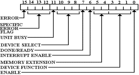
The
significance of bit 15 being the ERROR bit is that, in 16–bit arithmetic, it is
the sign
bit. Thus, the contents of the register
could be transferred to a general purpose register and
tested as if it represented a signed integer.
If negative, an error has occurred.
All devices
set bit 15 if an error occurred. Some
devices used bits 14 – 12 to indicate
specific errors; in this case bit 15 was the logical OR of bits 14–12.
Bit 11 was
generally used to indicate that the unit was busy. For output devices, this indicated
that the device could not accept data for output just at that time.
Bits 10 – 8
were used when the device controller was attached to multiple units. For example,
a disk controller might control multiple disks.
The 3 bits would select up to 8 devices.
Bit 7 is
the DONE/READY bit. If set, the device
is ready for another data transfer.
Generally speaking, bits 11 and 7 should not both be set at the same time.
Bit 6 is
the Interrupt Enable bit. When set, the
device will raise an interrupt when it has
completed a function or whenever an error condition occurs. An interrupt allows an I/O device
to signal the CPU. We shall discuss
interrupts and interrupt driven I/O very soon.
Bits 5 and
4 were used when the device would transfer data directly to or from main
memory.
This was required to support the memory management unit.
Bits 3 – 1 were used to specify the specific function to be executed.
Bit 0, when set, enables the device to perform I/O.
Sample Code for Paper Tape Input
The
following is a sketch of code for reading a single character from the standard
paper tape
reader on a PDP–11. For those very few
in the know, this is the paper tape reader associated
with the Teletype device, not the high–speed paper tape reader.
This is
written in a pseudocode, using all upper case letters. We follow the C++ and Java
convention in using the double slash “//” to denote comments. The prefix “0X” is used to
denote hexadecimal values; thus 0X41 is the hexadecimal
representation of decimal 65.
#DEFINE
TKS 0X3FF70 // DECIMAL 262,000
// ADDRESS OF
STATUS REGISTER
#DEFINE
TKB 0X3FF72 // DECINAL 262,002
// ADDRESS OF
DATA BUFFER
//
IN WHAT FOLLOWS, WE MANIPULATE BITS 0, 6, AND 7 OF THE
// STATUS REGISTER TKS. THE FOLLOWING
HEX VALUES ARE USED
//
0X41 (BINARY 0100 0001) SETS BITS 0 AND 6
// 0X80 (BINARY 1000 0000) ISOLATES BIT 7
READ: MOV 0X41, TKS // SET READER ENABLE AND
// INTERRUPT
ENABLE
LOOP: MOV TKS, R0 // GET STATUS VALUE INTO REGISTER 0
AND R0, 0X80 // EXAMINE BIT 7 OF TKS, NOW IN R0
BZ
LOOP // IF VALUE IS 0,
BIT 7 IS NOT SET
// AND CHARACTER
NOT IN BUFFER
MOVB TKB, RO // MOVE THE BYTE IN BITS 7 – 0 OF
// THE BUFFER
TKB INTO REGISTER R0
RET // AND RETURN.
This is a
pseudo–assembly language representation of polled
input. This is very inefficient.
This is the polling mechanism that Rob Williams [R004, p194] calls “dedicates spin polling”.
While the program waits for the input character to become ready in the input
data buffer, it
does nothing else. This is a great waste
of resources.
Rob
Williams [R004, p194] suggests another polling mechanism that is somewhat less
inefficient. This he calls “intermittent timed polling”, referring
to a mechanism in which the
CPU will spend some time in the dedicated polling loop and then execute another
program for
a fixed amount of time before resuming the polling loop. The advantage of this is that the CPU
does some useful work while waiting for very slow input. The disadvantage of this method is
that the processing of the input might be delayed until the polling resumes following
the
execution of other code.
What is
needed is a method by which the I/O device can signal the CPU when it is ready
to
transfer data. This will be developed in
the mechanism called an interrupt.
Before we
leave this discussion, we should mention two more topics: one serious and
related to
all polled input, and another frivolous and related to paper tape readers,
The serious
topic is based on some code taken verbatim from Rob Williams’s textbook
[R004, p 192]. This relates to a number
of serious topics in C or C++ coding, and possibly
in Java coding. Here is the code
fragment.
do {
while (!(*(BYTE *)RXSTATUS & RXRDY)) {} //wait until data arrives
} while (*pch++
= *(BYTE *)RXDATA) ; //check for
NULL
The first
comment has to do with the stylistics of “sophisticated” C and C++
programming.
In this nested pair of while loops, the body of the loop
is { }; it does nothing. The action is
to be found in the while conditions.
The curious
notation (*(BYTE
*) in each of the while loops is required by the compiler to
convert data types. The (BYTE
*) converts from an integer type to a pointer to a byte, as the
registers in this example are all 8–bit registers. The leading * in the (*(BYTE
*) converts
the pointer to its reference value, a byte, by a process called dereferencing.
A similar
example of dereferencing can be seen in the *pch++
construct in the outer loop.
The pointer value pch is incremented and the
character defined by *(BYTE *)RXDATA) is
stored at that address. Note that the
expression (*pch++ = *(BYTE *)RXDATA)
returns a
value, the ASCII code for the character just retrieved. When this character is NULL, with ASCII
value 0, the end of input has been reached and the while loop
terminates.
The
function of the embedded while loop is to delay until the
status register RXSTATUS
indicates that there is another character in the data buffer, ready to be
read. For the PDP–11,
this would be the same as TKS & 0x80, masking and
testing the DONE bit. For
a proper
reading of this embedded loop, one should refer to a C++ book, such as the
textbook by
D. S. Malik [R028, pp. 1175 – 1176]. The
expression to consider is repeated in the line below,
just below an extra comment line used in pairing the parentheses.
// 1 2 3 3 2 1
(!(*(BYTE *)RXSTATUS & RXRDY) )
In this
light, the expression is of the form !(Something),
looping as long as the expression
evaluates to TRUE (not 0). This is
equivalent to looping as long as Something is
FALSE (0).
This Something expression is *(BYTE
*)RXSTATUS & RXRDY). A
proper interpretation
of this expression is based on the relative precedence of the operators. In this expression,
1. The
type cast operator (BYTE *) has the highest priority,
so that the integer represented
by RXSTATUS is first
converted to a pointer to a byte.
2. The
dereference operator has the next priority, so that *(BYTE *)RXSTATUS is
interpreted as a byte
value. We might call it bStatus.
3. The
bitwise AND operator & has the
lowest priority. It is the mask for the
READY bit in the RXSTATUS
register.
If 0 == bStatus
& RXRDY, there is no character ready to be read. In this case,
!(*(BYTE *)RXSTATUS &
RXRDY) evaluates to True, and the loop continues.
When a character is ready for transfer,
the expression bStatus & RXRDY
evaluates
to 1, and !(*(BYTE *)RXSTATUS &
RXRDY) evaluates to 0, terminating the loop.
The reader
will note one major difference between C++ and Java. In each of C and C++,
the Boolean values are interchangeable with integer values; 0 is evaluated as
FALSE and
(not zero) is evaluated as TRUE. The
Java programming language makes a distinction between
Boolean and integer values. The
construct above, abbreviated as
do while (!(*(BYTE *)RXSTATUS & RXRDY)) {}
would not compile in Java. It would have to be rewritten something like the following.
do while (0 != (*(BYTE *)RXSTATUS & RXRDY)) {}
To a casual
reader, neither of the above constructs makes any sense, above and beyond the
fact that the identifiers RXRDY and RXSTATUS are written in all capital letters. The standard
usage in both C++ and Java is to use lower case letters for variables. The point here is that
neither RXSTATUS nor RXRDY
is a variable in the strict sense.
Consider
either of the loops above under the assumption that both RXRDY
and RXSTATUS are
variables. Note that nothing in the code
within the loop changes the value of either.
How then
can the loop exit, if it is even entered.
One of the standard compiler optimizations is the removal
of loop invariants from a loop, to avoid needlessly repetitious
evaluations. Consider this loop.
for
(j = 0, j <= 10, j++)
{ x = 5 ;
y = 7 ;
a[j] = x*a[j] + y;
} ;
Any
standard compiler would replace that loop with the following. Note that the loop
invariant code has been moved to statements before the loop.
x =
5 ;
y = 7 ;
for (j = 0, j <= 10, j++)
{ a[j] = x*a[j] + y ;
} ;
But neither
RXSTATUS nor RXRDY
is a variable. A true variable receives
its value as a result
of execution of the program and assignment by the CPU. Here each of RXRDY
and RXSTATUS
represents a register that has values set by I/O hardware. In other words, the loop
do while (!(*(BYTE *)RXSTATUS & RXRDY)) {}
is likely to terminate despite the fact that no program statement will cause
either value to change.
Identifiers
with this property are classified as volatile
in both C and C++. This informs the
compiler that these two identifiers may appear to be program constants, but in
fact are being
changed by external action. The compiler
will emit code to cause each of the identifiers to be
evaluated for each execution of the body of the loop.
Silly Paper Tape Story
Is it
possible to destroy a compiler? Yes, if
the compiler is stored on paper tape. In
1964,
your author was running a FORTRAN program on an IBM 1620. Part of that required
loading the compiler from paper tape and then loading the text of the program
likewise.
Your author stepped on the paper tape, and the high speed reader tore the tape
into shreds;
the compiler was destroyed. Fortunately,
we had many back–up copies.
Bus Signaling
The next
logical step in the presentation of input and output will be the discussion of interrupt
processing, also called “interrupt
driven I/O”. This is an evolution of
polled I/O in which the
device will signal the CPU when it is prepared to transfer data (either in or
out). This discussion
will be greatly facilitated by a brief, and possibly duplicative, discussion of
bus signaling.
We first
ask about signal assertion; how is a signal placed on a bus line. The most common
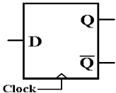
method involves some sort of D flip–flop, either a latch or a true
flip–flop. While there may be
some obscure timing issues that favor the use of a latch over a flip–flop, we
shall assume and
explain the use of a D flip–flop.
The basic
idea of a flip–flop was discussed in Chapter 6 of these notes. As noted then, the
flip–flop is a synchronous sequential circuit element. As a synchronous
circuit element, it
changes states in response to a clock signal.
As a sequential circuit element,
it represents
memory, as it is a form of data storage.
Here are two figures, copied from Chapter 6.
The D flip–flop just stores whatever input it had at the last clock
pulse sent to it. Here is one standard
representation of a D flip–flop. The
design scenario for which this is used is simple:
the CPU asserts a value for a brief time, and the flip–flop stores that value
until it is changed.
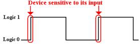
When D = 0 is sampled at the rising edge of the clock,
the value Q will be 0 at the next clock pulse.
When D = 1 is sampled at the rising edge of the clock,
the value Q will be 1 at the next clock pulse.
This D flip–flop just stores a datum, a single bit.
The next question is how to prevent this device
from loading a new value on the rising edge of
each system clock pulse. We want it to
store a
value until it is explicitly loaded with a new one.
The answer is to provide an explicit load signal,
which allows the system clock to influence the
flip–flop only when it is asserted.
It should be obvious that the control unit must
synchronize this load signal with the clock.
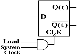
In keeping
with standard design practice, we shall use the Q(t) output of the flip–flop to
drive a bus line, and not use the other output.
We just do not need the complement.
The set of
D flip–flops form part of the interface between the CPU and the I/O bus. These
flip–flops allow the CPU to assert addresses that will be permanently available
on the bus
until used. There are D flip–flops used
for input to the CPU. For these the
input device will
place data into the set of flip–flops for later use by the CPU, which will
access the data when
the program allows.
We begin
our discussion of an output interface D flip–flop with the simplest possible
case. This
is a D flip–flop without a load signal.
It accepts input on the rising edge of each clock pulse.
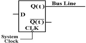
Here is a figure showing the action of a flip–flop that is triggered on the rising edge of the clock.
We now
examine a very simplistic, almost inaccurate, figure to make a point about the
relative
timings of the clock and the data input.
Consider the following timing diagram.
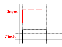
The problem
arises from the fact that the input (D) to the flip–flop changes at the same
time
as the rising edge of the clock. This
can give rise to a race condition,
in which there is no
guarantee which value will be stored. To
say that the results of storing the wrong value can be
deadly may seem dramatic, but this has happened.
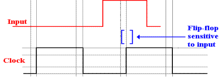
What is
required is to have the input to the flip–flop stable for a time before the
rising edge of the
clock and for a specific time after that rising edge. The next figure suggests a proper timing.
The proper timing, with the use of the LOAD signal, is shown below.
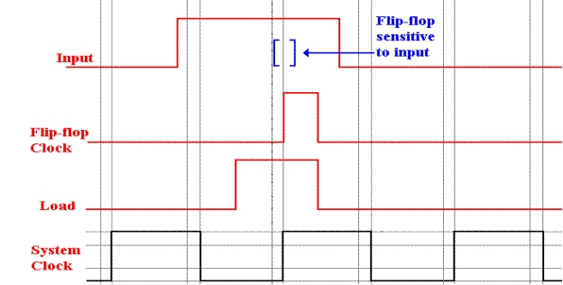
The first
thing to note in this timing diagram is that the signal Flip–Flop Clock (the
clock input
to the flip–flop) is the logical AND of the Load Signal and the System
Clock. The high part of
the Load signal must overlap the high part of the clock signal for a time
sufficient to cause the
flip–flop to load. Note the relative
timing of the input and the Flip–Flop clock.
The input must
be stable for some time before the Flip–Flop Clock goes high and remain stable
for some time
after that signal goes high. Note that
the contents of the D flip–flop will remain constant until
such time as the Load signal is again asserted.
Timing Considerations
Most
introductions to computer organization do not cover timing considerations, as
they can be
quite complex with subtle race conditions.
As noted above, a race condition
might occur when
the relative timing of two or more signals is important and not possible to
guarantee. We have
seen in the above a case with three signals: System Clock, Load, and
Input. The strategy here
is to allow generous overlap, so that the input is properly stored in the
flip–flop.
The goal of
this course is to lead to an appreciation of the importance of timing in
digital circuit
design and to indicate some simple solutions.
A complete study of timing considerations would
be the subject for a more advanced course.
Assertion of Signals on Bus Lines
Consider
any device with output connected to a bus line.
Our example of this is a D flip–flop
with Q output connected to a bus line.
The output will be either logic 1 or logic 0. When the
output of a D flip–flop is connected to a line, it is said to be asserted on that line. We now
discuss two methods for signal assertion by a source, such as a flip–flop.
1. Direct connection of the output.
2. Connection through a tri–state buffer.
In direct
connection, the output of the source is directly connected to the bus
lines. For a single
bit value being asserted on a single bus line, we have the following diagram.
This design
is useable only in those cases in which there is exactly one source of value to
be
placed on the bus line. An example of
this might be a set of address lines in the case in which
there is only one bus master (a
device that controls the bus) allowed to set the address.
In the case
in which there are two or more sources possibly driving the bus line, each is
connected to the bus via a tri–state buffer.
Recall that a tri–state buffer either passes its input
to its output, or does not assert anything on its output line. Here each of the tri–states is shown
as enabled high; when A ® Bus = 1, the value in the flip–flop for Source A is
asserted on the
bus. When A ® Bus = 0, the output for
the top tri–state is not defined.
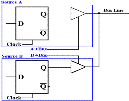
The action of this circuit is described by the following table.
|
A ® Bus |
B ® Bus |
Action |
|
0 |
0 |
Neither source asserts a value; the bus “floats”; i.e., no value is defined. |
|
0 |
1 |
Source B determines the value asserted on the bus. |
|
1 |
0 |
Source A determines the value on the bus. |
|
1 |
1 |
This is an error condition, possibly a short–circuit. |
There is
another, more specialized, use of tri–state buffers to define a signal on a bus
line. The
situation above contemplates connection of the output of a flip–flop to a bus
line; the binary
value stored in the flip–flop is asserted onto the bus. In this next example, taken from design
of I/O interrupt circuitry, the goal is to assert a logic 0 on the bus line.
In order to
understand this use of tri–state buffers, it is helpful to begin with the
following
circuit, which is more fully explained in the appendix to this chapter.
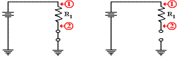
What is the
voltage at points 1 and 2 in each circuit?
In each circuit, the voltage at point 1
is the full voltage of the battery, let’s call it V. But what about point 2?
In the
circuit at left, the switch is closed and connects point 2 directly to
ground. The voltage at
this point is 0, with the entire voltage drop across the resistor. The resistor is sized so that only a
small current flows through it in this situation.
In the
circuit at right, the switch is open and acts as if it were a very large
resistor. The result,
explained in the appendix to this chapter, is that the voltage at point 2 is
also the full battery
voltage. Because the switch acts as such
a large resistor, there is no voltage drop across R1.
We now
consider another circuit, also explained in the appendix to the chapter. This connects
a number of switches to the circuit above.
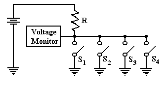
If all of
the switches are open, as shown in the figure above, the voltage at the monitor
is the
full battery voltage. If one or more of
the switches is closed, then the voltage monitor is
connected directly to ground, and the voltage at that spot is zero.
The key
design feature for this and similar circuits is that there can be no conflict
between any
two switches. Either a switch is
connecting the reference point to ground, or it is doing nothing.
Specifically, no switch is connecting the reference point to any voltage
source. If the resistor R
is sized properly, this circuit cannot cause any problems.
Realizing
that the tri–state buffer is just a fancy switch that is electronically
operated,
we come to the following circuit for driving a bus line to ground. Each box is associated
with some sort of I/O device, and controls one of the tri–state buffers. When one control
box is active and enables its tri–state buffer, the voltage at the reference
point is driven to
zero; this can be tested by the monitor and used as a signal.
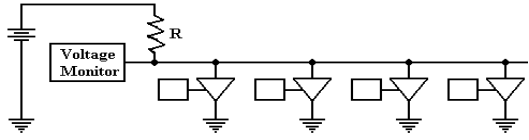
The same
thing happens when two or more of the control boxes are active. When there are
no control boxes active, and no tri–states enabled, the voltage at the
reference point is the full
battery voltage. This also can be tested
by the monitor and used as a signal.
Strobed Signaling
By
definition, a bus transaction
requires a data source asserting signals on a bus and a data
consumer copying those data from the bus.
For a data input, the data source (say, a paper tape
reader) will place data onto the bus and the CPU will copy those bits into an
internal buffer. A
necessary part of this transaction is the determination of when the data are
valid.
Consider
the paper tape reader example, under the very unrealistic assumption that it
can
produce data upon command. Assume 8 data
lines on the I/O bus. For a synchronous bus,
the design is such that the data can be assumed to be on the data lines after a
fixed known delay
following the assertion of the read command on the bus.
For an asynchronous bus, the data source must
assert a strobe signal to indicate that valid data
have been placed on the data lines.
Here, we assume a signal DS#,
asserted low by the reader,
to signal the CPU that it may accept the data as valid. Here is a timing diagram, with
timing marks shown for the sake of discussion.
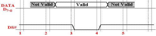
Some time after
T = 2 and before T = 3, the reader asserts valid data onto the data lines, D7–0.
At T = 3, the reader asserts the data strobe DS# by driving it to 0. This
signals the CPU that
the data on the data lines are valid. At
T = 4, the reader ceases to assert the data strobe, and it
returns to logic 1. This indicates that
the data lines very soon will no longer be valid.
Consider
the notation for the data lines. Unlike
the DS# line, it is not possible to
specify the
binary value on any data line. Our only
concern is that valid data are present; hence the notation.
Interrupt Processing
It should
be obvious that I/O would be more efficient if the CPU did not have to wait for
the
I/O device to become available. If it were possible for the I/O device to
signal the CPU when
it was available for data transfer, the code for the actual transfer could be
executed efficiently.
An interrupt is almost always an
externally generated signal to the CPU that causes it to
suspend normal processing and execute code to handle the interrupt. Interrupts arise naturally
within the context of input and output; this is the context within which we
shall discuss them.
Other types of interrupts include page faults (see Chapter 12 – The Memory
Hierarchy) and
execution traps, such as arithmetic overflow or division by zero.
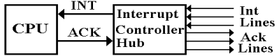
At the top
level, interrupt processing is managed by two components of the computer: the
CPU and an ICH (Interrupt Controller Hub).
On designs built around the Pentium, this
control hub is generally called the PIC
(Programmable Interrupt Controller). The division
of work is suggested by the figure below.
The normal
design allows for many devices that might interrupt the CPU and cause special
code to be executed. To allow for proper
handling of urgent processing, each device is assigned
an interrupt priority. This design
prevents low priority tasks from preempting high level tasks.
On the PDP–11, interrupts are assigned eight priority levels: 0 through 7. The disk is assigned
priority level 7 and asserts its interrupt on the line INT7, the line for that
priority. The keyboard,
paper tape reader, and paper tape punch are assigned priority level 4. Other devices are assigned
priority levels 5 and 6; by design all I/O interrupts have priority at least 4.
One basic
mechanism for managing I/O interrupts is based on CPU execution priority. The
CPU has an entry in the PSR (Program Status Register) indicating the priority
of the program it
is executing at the time. User programs,
by definition, execute at priority level 0.
The standard
practice calls for running a device handler at the priority for the device;
thus the device driver for
the disk (priority level 7) executes at priority level 7, and that for the
keyboard (priority level 4)
executes at priority level 4.
One
standard design rule for handling interrupts is that the CPU will process an
interrupt if and
only if the interrupt priority exceeds the CPU execution priority. Thus, a user program may be
interrupted by either a keyboard interrupt or disk interrupt, the keyboard
device driver (handler) may be
interrupted by a disk interrupt (but not a paper tape reader interrupt – same
priority), and
the disk device driver may not be interrupted, as it has the highest priority.
The division
of work between the ICH (Interrupt Control Hub) and the CPU is illustrated by
the
two signals between the two. These are
the INT signal raised by the ICH and the ACK signal
raised by the CPU. The INT signal is
asserted by the ICH if and only if there is a device
interrupt of sufficient priority to be handled.
The CPU responds to this signal by completing
execution of some code, starting a general interrupt handling routine, and
asserting the ACK.
The ACK allows the ICH to send an acknowledge signal to the appropriate device.
In what
follows, we again use the PDP–11 as an example.
As mentioned above, there are four
priority levels reserved for I/O devices: 4, 5, 6, and 7. Each priority level has an associated INT
(device interrupt) line and ACK (device acknowledge) line; INT7 and ACK7 for
level 7, etc.
This
discussion will also use the PDP–11 assertion levels; all interrupts are
asserted low, and
all acknowledge signals are asserted high.
In the more modern notation: INT7# and ACK7.
The main
function of the ICH is to process at most one interrupt at a time. The ICH may be
considered to have a number of components to facilitate this processing. The first is the priority
ranker for incoming interrupt signals.
The following circuit shows its function.
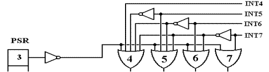
In this
part of the ICH, there are four possible outputs – one for each hardware
priority level.
The job of this is to handle multiple inputs and produce at most one output. If one of the outputs
of this bottom row of OR gates is asserted low, then that interrupt has passed
the first test.
We begin
with the fact that the CPU will enable interrupts by setting bit 3 of the PSR (Program
Status Register) to 1 and disable interrupts by setting the bit to 0. Suppose that PSR bit 3 is set
to 0. The output of the NOT gate is then
1, which is input to each of the four OR gates causing
each to output a logic 1. In other
words, no interrupt can pass the first filtering level if the CPU
has disabled interrupts.
Suppose now
that PSR bit 3 is set to 1. This causes
a logic 0 to be input to each of the OR gates,
allowing the output of each to depend on the values on the incoming INT
lines. The task at this
time is to pass at most one interrupt level.
If interrupts are asserted as two or more priority levels
only the highest priority will be passed.
Here are two cases to consider.
1. Suppose
no interrupt is being asserted. Then
each of INT4, INT5, INT6, and INT7 will
be set to logic 1. This causes the output of each of the four OR
gates to be 1. As no
output from this level is set
to 0, no interrupt is processed.
2. Supposes
that two interrupts are being asserted, one by a device at level 4 and another
by
a device at level 6. The inputs are INT4 = 0, INT5 = 1, INT6 = 0,
and INT7 = 1. Follow
the signals INT7 and INT6
through the circuit component. As INT7 =
1, the output of
the OR gate at this level is
set to 1, no interrupt is asserted at this level. In addition, the
output of the NOT gate
attached to INT7 is 0, allowing lower priority interrupts.
Now we look at the INT6 input. It is set to 0. The inputs to the priority level 6 OR gate
at the bottom are INT6 (logic
0) and NOT(INT7), also logic 0. Thus,
the output of this
logic gate is 0 and the
interrupt at this level can be processed.
Note that NOT(INT6) is
logic 1; this is input to the
OR gates for level 4 and 5, forcing the output of each to 1.
Specifically, the output of OR gate
4 is 1 and the INT4 is ignored for the moment.
The
device will continue to assert
the interrupt, which will be handled when INT6 goes to 1.
The next
step compares the priority of any interrupt passed to the execution priority of
the CPU.
The execution priority of the CPU is stored as a 3–bit unsigned integer in bits
2, 1, and 0 of the
PSR. If the incoming priority is greater
than the execution priority, the interrupt is allowed.
Here is a conceptual schematic of this stage.
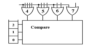
Suppose the
execution priority is 5, stored as 101 in the PSR. If the output of OR gate 6 is 0,
indicating an admissible interrupt at that level, it will be allowed. If the output of OR gate 5 is
0, then the interrupt is not allowed, as the CPU is executing at that priority
already. Note that
the first circuit is designed so that at most one of the OR gates will have an
output of 0. By
design if the output of OR gate 5 is 0, then the output of the other OR gates
must be 1.
If the
interrupt passes muster at this level, the INT signal to the CPU is
generated. When the
ACK signal returns from the CPU, the ICH (Interrupt Control Hub) passes down
the appropriate
ACK line and the interrupt processing begins.
There is
only one more detail to handle at this level.
There may be more than one device on a
given level. For example, priority level
4 on the PDP–11 is used by the keyboard, paper tape
reader, and paper tape punch. How does
the appropriate device get selected.
Multiple devices at a given level are handled by what is called a “daisy chain”.
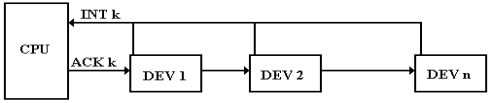
In the
daisy chain, the ACK signal is sent to each device on that priority level in
turn. If
the device has raised an interrupt, it captures the ACK and begins interrupt
processing. If
the device has not raised an interrupt, it passes the ACK to the next device.
As an
example, assume four devices with DEV 1 closest to the CPU. Suppose that DEV 2
and DEV 4 have raised an interrupt. The
ACK at this level is passed down.
1. It is passed first to DEV 1. As this has not raised an interrupt, it passes it to DEV 2.
2. The
ACK is passed to DEV 2. This captures
the ACK and does not pass it on to
DEV 3. Thus DEV 4 does not get the ACK until DEV 2
has processed its interrupt
and dropped its INT.
There is one caution here: do not place too many devices on a given level.
Identifying the Device
When the
CPU accepts the INT signal from the ICH (Interrupt Control Hub), the next step
is to identify the device that raised the signal so that it might be
handled. At this point, the
only information available to the CPU is that some device raised the interrupt,
and that it
had the proper priority to do so.
We have traced the first steps in this process in the above discussion. Here is what happens.
1. The CPU issues the ACK (Acknowledge) signal to the ICH.
2. The ICH converts the ACK to an acknowledge on the proper line, say ACK4.
3. The
interface hardware for the device captures the ACK on its line.
Here, let us suppose it is the
keyboard.
How is the
device identified to the CPU so that the proper device handler software can be
run?
There are a number of methods possible, but we describe the one that is most
commonly used.
It is called a “vectored interrupt”. In this design, the hardware interface that
captures the ACK
responds by placing its vector onto
the data lines.
The vector
is an address; more specifically, it is an offset into the IVT (Interrupt Vector Table).
In some of the earlier computers, such as the PDP–11 and Intel 8086, this
vector was an absolute
address, commonly in low memory.
Typically, it might have a value such as 0x18, referencing
address 0x18 or decimal 24 in primary memory.
In other words, this was an offset into the IVT,
which was loaded at address 0 in primary memory; offsets became actual
addresses.
More modern
operating systems are built upon tables of data that can be loaded anywhere in
main memory. For interrupt processing,
the base address of the IVT must be tracked so that the
absolute address of the word indicated by the offset can be computed. In the Pentium designs,
the base address of the IVT is stored in the IDTR (Interrupt Descriptor Table Register).
As an
example, consider a possible IA–32 configuration, in which each entry in the
IVT is a
32–bit (four byte) address. All byte
addresses in this table must be multiples of 4.
Suppose
that the base address of the IVT is 0x0260, and that the device vector is
0x18. This
references an entry in the IVT at offset 0x60 (0x18 · 4 = 0x60, in decimal 24 · 4 =
96). What
we have is seen in this calculation. In
hexadecimal 6 + 6 = C; in decimal 6 + 6 = 12.
Contents of the IDTR 0x260
Offset address 0x060
Computed address 0x2C0.
The 32–bit
value stored at address 0x2C0 is the address of the
software to handle the interrupt.
In vectored interrupts, the device does not identify itself directly, but points
to the device handler
software to process the interrupt.
The general software for handling interrupts has at least three parts.
1. The
software to load the interrupt handler into main memory and to initialize the
address in the vector. This is done by the OS loader.
2. The operating system I/O routine that is called by the user program, and initiates the I/O.
3. The interrupt handler routine that actually processes the I/O.
Note that
the software associated with any given I/O device is divided into parts that
are
not commonly located in adjacent memory or executed sequentially. This makes reading the
system code more difficult; a task made tolerable only because it is so rarely
necessary.
It is
possible to give examples of old PDP–11 code at this point, but such an example
would
obscure the main point of interrupt processing.
The example code available in the handbooks
calls for the user process to stall awaiting the input, and for the CPU to do
nothing else while
awaiting the input interrupt. Such a
situation is hardly better than dedicated spin polling.
In order to
understand the significance of interrupt–driven I/O, it is helpful to place it
within
the context of process management by the operating system. Because the concept is so basic
to the execution of a program, the concept of a process is a bit hard to define
exactly. One good
definition is that a process is a program in execution; when a program is
executing, its process is
active. One may also define a process as
the collection of data structures necessary for the
associated program to execute, but that leads to topics that are not relevant
here.
Process
Management
The best
way to illustrate process management by a modern operating system is to discuss
a
strategy, called “time sharing”,
used in computers with many users. One
example of this is
the IBM Mainframe used for teaching at Columbus State University. At any time, there are
a few tens, perhaps hundreds, of users each using a video terminal to run a
program on the
computer. Each user gets good service,
appearing to be the only one using the computer.
In the Time
Sharing model, we have
1. A
single computer with its CPU, memory, and sharable I/O resources,
2. A
number of computer terminals attached to the CPU, and
3. A
number of users, each of whom wants to use the computer.
In order to share this expensive computer more fairly, we establish two rules.
1. Each user process is allocated a “time slice” or “quantum” during which it can be run.
At the end of this time, it must
give up the CPU, go to the “back of the line” and
await its turn for another time
slice.
2. When a process is blocked and waiting on
completion of either input or output,
it must give up the CPU and cannot
run until the I/O has been completed.
Here is the standard process diagram for a program being executed in a time sharing mode.
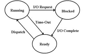
The ready state contains process
information on all programs that are ready to run, but have
not yet been given control of the CPU.
When a program is dispatched,
it begins execution.
There are two ways in which a program can leave the running state. For each of
these options,
the goal of the operating system is to dispatch another process in order to
keep the CPU busy.
If the
running process reaches its time allocation, and there is another process ready
to run, the
operating system times it out and the process reverts to the ready state. The process still has all
of the resources necessary to run, but the operating system must “play
fair”.
The situation
of interest here occurs when the process requests I/O or some other resource
that
cannot immediately be granted. At that
point, the process is marked as blocked,
and another
process is allocated the CPU. During
this time in which the process is blocked, the operating
system will be managing the I/O, using interrupts. When the I/O is finished, the process is
marked as ready to run, and will run as soon as its turn arrives.
There are
three “players” in this game: the user program, the I/O management system of
the
operating system, and the device driver for the I/O hardware. The following scenario shows
possible interactions for the three, when the string “INPUT” is input via
a standard read.
1. The
user program uses a predefined system routine, perhaps scanf(),
to
begin the I/O process. On modern operating systems, I/O is managed
by the operating
system running in privileged
mode, so the user program cannot do this directly.
2. The
executing code creates a data structure representing the request and issues a SVC
(Supervisor Call) or trap to invoke the services of the
operating system. On an IA–32
system, this might be
interrupt 21H (33 decimal) with the AH register set to code
07H or 0AH. The main difference between a SVC and
standard procedure call is that
the SVC allows the called code
to run in privileged or kernel mode.
3. The
user program is blocked. The I/O
management system creates a buffer for storage
of the input, enables the
appropriate interrupt, and then blocks itself.
4. The
process manager schedules another process to run on the CPU, awaiting the
completion of I/O for the
blocked process.
As each of the six characters (five alphabetical and the EOL character), the following occurs.
5. The
input device raises an interrupt, causing the operating system to suspend the
executing program and run a
process to retrieve the character. It is
placed in the
buffer managed by the blocked
I/O process for the blocked user process.
6. The
I/O management system re–enables the input interrupt. The suspended
process is resumed. The blocked user process remains blocked.
When the
EOL character (ASCII code decimal 13) is entered, the processing is as above,
except that the I/O management process remains unblocked and delivers the
string “INPUT”
to the blocked user process.
7. The blocked user process is marked as ready to run.
It is
important to note that the CPU is directly involved in the transfer of each of
the six
characters. There are six input interrupts,
six invocations of the handler software, and six
invocations of the I/O management process.
One way to
examine interrupt–driven I/O as opposed to program managed (polling) I/O is
to examine the amount of code executed for each. It will soon become obvious that the
interrupt–driven approach involves more code, and more complex code, than the
polled
method. The advantage is that the CPU
does not stall, awaiting the I/O.
Put another
way, the user program stalls, but the CPU is kept busy executing other
processes.
This approach increases productivity in a time–sharing mode, in which the main
measure is
number of programs competed per time unit.
Each program might take longer to execute than
if it were run with program controlled I/O, but a reasonable system makes the
difference small.
DMA (Direct Memory Access)
In
interrupt–driven I/O, each character is directly transferred by the CPU. The next step would
be to provide the I/O device hardware with the ability to manage main memory
directly, and
thus accomplish the I/O with very little involvement from the CPU.
As we have
seen, the CPU interacts with main memory via two registers (MAR and MBR) and
a pair of control signals. In DMA, the
I/O device hardware can place an address in the MAR,
possibly data into the MBR, and then issue the appropriate memory
commands. On a balanced
system, the CPU and I/O devices share control of the memory.
Suppose
that a disk drive is set to transfer a 512–byte block of data. This is the size of a disk
sector on many disks. Were this transfer
managed by interrupt–driven I/O, there would be
513 interrupts generated, one to start the process and one for each of the 512
characters. DMA
does the same job with only two interrupts.
Here is the scenario.
1. The disk asserts an interrupt indicating that data are ready to transfer.
2. The operating system responds by activating the disk handling software.
3. The
disk handling software sends the following to the disk managing hardware
a) A starting memory address for a 512–byte buffer to hold the
data.
b) The expected byte count for the transfer, here it is 512.
c) A signal to begin the I/O.
4. When
the I/O competes or an unrecoverable error occurs, the disk hardware
asserts the second interrupt.
5. The operating system interprets the completion code and responds accordingly.
I/O Channels and Such
The last
strategy to mention is not really a true strategy, it is the assignment of
another computer
to manage all of the I/O. On the CDC
series of supercomputers, such a device was called a PPU
(Peripheral Processing Unit). On an IBM
Mainframe, it is an I/O Channel.
One early
example is seen in the 1960’s with the IBM 1401/7094 combination. The IBM 7094
was the supercomputer of its day. It was
very fast on numerical computations, but lacked most
I/O facilities. The IBM 1401 was a poor
number cruncher, but it excelled at I/O.
The two were
paired together to form a complete computing system.
The IBM I/O
Channel concept reflects a style of computing called “enterprise computing”. In
this scenario, large volumes of data are processed using rather simple
algorithms. Efficiency in
I/O is the key, hence the dedicated I/O processors.