This
chapter will cover a number of topics related to sequential transmission of
data. We begin
with the problem of encoding data for transmission. This might be surprising; why not just
encode everything in ASCII and send it.
There is the minor issue of EBCDIC, used on IBM
mainframes; that is just another encoding.
The transmission of printable characters (with ASCII
encodings between 32 and 126 inclusive), this is the complete solution. The issue arises in the
transmission of binary data, such as MP3 files or pictures. Any file, textual or binary, can be
broken into bytes for transmission one byte at a time. This is called “serialization”.
The
main difficulty with the transmission of arbitrary binary data relates to the
early history of
serial data transmission, in which one or both of the communicating nodes might
be a classical
ASR33 teletype. We begin by discussing a
simple error detection method.
In
the early days of data transmission, many different encoding methods were used
to transmit
textual data. Given the desire to
transmit at least 36 different characters (26 alphabetic and 10
digits), not to mention punctuation, it was obvious that a 5–bit encoding would
not suffice;
25 = 32, and 5 bits would encode only 32 different symbols. For some time, 6–bit encodings
were used. The desirability of
transmitting lower case alphabetic characters and transmission
control characters quickly made this encoding obsolete.
The
next obvious choice was a 7–bit code; 27 = 128, allowing for the
encoding of 128 distinct
characters. This worked rather well, and
persists in the standard 7–bit ASCII. As
8–bit bytes
were becoming a popular memory organization, it was decided to add a parity bit
to the 7–bit
code in order to pad it out to 8 bits and allow single–bit error detection.
The
parity of an 8–bit datum is based on
the count of 1 bits. If that count is
even, the parity is
said to be even. If that count is odd,
the parity is said to be odd. The
transmission standard will
be either even parity or odd parity. The
parity bit is set based on the count of 1 bits in the 7–bit
code. If the 7–bit ASCII has an even
number of 1 bits, the parity bit is set to 1 so that the total
will be an odd number. If the 7–bit
ASCII has an odd number of 1 bits, the parity bit is set to 0.
Here
are some examples, based on upper case alphabetical characters.
|
Character
|
7–bit ASCII
|
Even Parity
|
Odd Parity
|
|
‘B’
|
100 0010
|
0100 0010
|
1100 0010
|
|
‘C’
|
100 0011
|
1100 0011
|
0100 0011
|
|
‘D’
|
100 0100
|
0100 0100
|
1100 0100
|
|
‘E’
|
100 0101
|
0100 0100
|
1100 0100
|
In general,
there is little reason to favor one method over the other; just pick one and
use it.
One minor consideration is the encoding of the ASCII NUL (code = 0) for 8–bit
transmission;
in even parity it is “0000 0000”, while in odd parity it is “1000 0000”, at
least a single 1 bit.
Here
is the second bit of history to consider before moving on to consider data
transmission.
This is due to the heavy use of transmission control characters in the early
days. Here are a few:
|
Character
|
Keyed
As
|
7–bit
ASCII
|
Comment
|
|
EOT
|
^D
|
000
0100
|
Indicates
end of transmission.
|
|
NAK
|
^E
|
000
0101
|
Data
not received, or received with errors.
|
|
DC1
|
^Q
|
001
0001
|
XON:
Resume transmission.
|
|
DC3
|
^S
|
001
0011
|
XOFF:
pause transmission. The receiver
buffer is full; new input data cannot be processed
|
So
say that these design features have been “hardwired into the design” of most
transmission
units is to speak literally. It is a common
design practice to implement functionality in hardware,
rather than software, if that functionality is frequently needed. The increase in efficiency of the
unit more than pays for the increased cost of the hardware.
Given
these two facts, now consider what will happen to a general binary file if it
is serialized
into 8–bit bytes and transmitted on byte at a time. It is likely that about 50% of the bytes
arriving at the receiver will be rejected as having the wrong parity.
Suppose
the receiver in a two–way connection receives the binary pattern 0001 0011, the
8–bit odd–parity encoding of the DCE 3 (XOFF) character. It will promptly cease data
transmission back to the source until the DCE 1 (XON) character is received, an
event that
is not likely as the sender has stopped transmission. While this feature is useful in managing
transfer to and from a video terminal, here it is a real problem.
COMMENT: Many students taking courses that require
access to an IBM mainframe will
find the code “XMIT BLOCK” displayed on the screen. One way that might resume data
transmission is to use the Control–Q option, sending the XON character to the
mainframe.
The
issue of sending raw binary over a serial link is most often seen in e–mail
attachments.
The MIME (Multipurpose Internet Mail Extension) standard was developed to handle this.
There are several methods for making raw binary data “safe to transmit”. All involve packing
three 8–bit bytes into a 24–bit integer, and then breaking it into four 6–bit
transmission units,
each of which is then expanded into 8 bits with the proper parity.
Note
that each 6–bit transmission unit, viewed as an unsigned 6–bit integer, has
value in the
range 0 through 63 inclusive. The UNIX
encoding scheme, discussed here, adds 32 to each
of these values to generate an integer in the range 32 to 95; ‘ ’ to ‘-’.
Consider
the 3–byte sequence 0001 0011 0100 0001 0101 0011.
As
a 24–bit integer, this is 000100110100000101010011.
As
four 6–bit units, this is 000100 110100 000101 010011.
Represent
each of these in 8 bits 00000100 00110100 00000101 00010011.
Add
32 to each 00100000 00100000 00100000 00100000.
Values
in range 32 to 95 00100100 01010100 00100101 00110011.
Adjust
for odd parity 10100100 01010100 00100101 10110011.
These
are the codes for $ T
% 7.
The
MIME standard calls for a text block describing the encoded content to precede
that
encoded content. As an example, we use
part of figure 10.3 from William’s book [R004].
Content-Type: application/gzip;
name=“book.pdf.gz”
Content-Transfer-Encoding: base 64
Content-Disposition: inline;
filename=“book.pdf.gz”
Timing
Synchronization: Frequency and Phase
At
this moment, we continue with the pretense that the transmitter sends a
sequence of 1’s and
0’s on the communication line, and ignore the actual signaling voltages. We examine the
problem associated with the receiver’s sampling of the signal on the line. Here we assume
that the line frequency is known and that the transmitter sends out pulses at
that frequency.
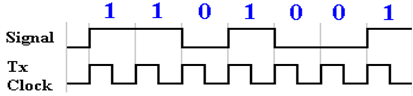
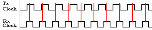
Here
is an idealized diagram of the situation at the transmitter for pattern
1101001.
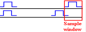
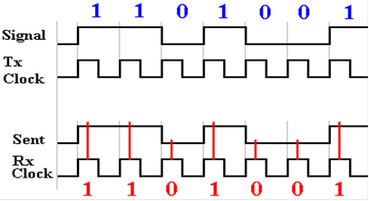
Ideally,
the receiver clock is synchronized with the transmitter clock. The receiver will sample
the line voltage in the middle of the positive phase of its clock and retrieve
the correct value.
But
suppose that the transmitter and receiver clock are not synchronized. Either they could
be operating at slightly different frequencies or at the same frequency, but
out of phase. The
more normal case is a difference in phase where the receiver samples at the
wrong time.
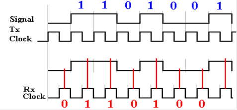
Here
the receiver clock is one half cycle out of phase with the transmitter
clock. One full
cycle is called 360 degrees, so this is a 180 degree phase difference.
All
designs call for the transmitter clock and receiver clock to have known
frequencies; here
we assume the same frequency. While the
crystal–locked oscillators in the clocks are quite
accurate, they are not perfectly so. For
example, as of December 29, 2011, the specifications
for the GX0–3232 listed a ±15 ppm (part per
million) frequency accuracy. Suppose
that the
transmit frequency is supposed to be 100 kilohertz. The real frequency might vary constantly
between 99,998.5 and 100,101.5 hertz (cycles per second). For this accuracy, one might
expect there to be a problem every (0.5/1.5·10–5)
= 33,000 clock pulses. What happens
is shown in exaggerated form in the figure below. The phase of the receiver drifts
with respect to that of the transmitter.
The
solutions that have been historically adopted have all involved periodic resynchronization
of the two clocks to prevent this drift in phase due to the very slight
frequency differences. The
most common solution remains in use today, because it works well and is easy to
implement.
The RS232
Standard
We
now look into details of a commonly used asynchronous communication protocol,
called
RS–232, as is commonly implemented. The
term “asynchronous” indicates that
no clock
pulses are transmitted, only data bits.
For this reason, it is important to have high quality
clocks on both the transmitter and receiver.
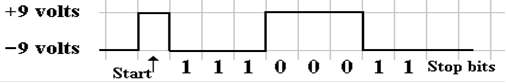
This
is a standard for transmitting binary information. The transmitter asserts a voltage
level on the transmission line to indicate the value of the bit being
transmitted. For the
RS232 standard, the levels are as follows:
–9 volts used
to transmit a ‘1’ bit. This is
called “mark” in the standard.
+9 volts used
to transmit a ‘0’ bit This is
called “space” in the standard.
In
this standard, each character is transmitted independently; thus, transmission
of a string
of characters will lead to a sequence of independent transmissions. Each transmission begins
with the line in the idle (mark) state, at –9 volts. To initiate a character transmission, the
line
is driven to the space state, at +9 volts, for one clock period. This is the “start bit”.
The
character is then transmitted, one bit at a time, with the least significant
bit first. Following
that, the line must remain idle for a fixed time. This period is denoted as 1 or more “stop bits”.
If the line must remain idle for two clock periods before the next
transmission, the standard is
said to call for 2 stop bits. If the
idle time is 1.5 clock periods, the standard is said to use
1½ stop bits, though there is no half bit sent.
The letter ‘G’, with odd parity, is encoded
as 11000111, and transmitted in reverse order, LSB first.
The
choice of the two voltages as negatives of each other is due to the desire to
have the
signal average at close to zero volts.
This minimizes the power transmitted across the line.
Error Detection and Correction
Errors
can occur in any sort of data that is stored or transmitted, either in analog
form or in
digital form. One of the benefits of the
digital forms is that many such errors can be detected
and some of them actually corrected.
This observation introduces the topic of error detection
codes and error correction codes.
Parity,
mentioned several times above, is the simplest form of error detection. While it is easily
and quickly applied, the parity will detect only single bit errors. Parity, by itself, provides no
mechanism by which errors can be corrected.
The
parity of a data item is based on the count of 1 bits in the encoding of that
item. If the count
is an odd number, the item has odd parity.
If the count is even, so is the parity.
The simplest
example of parity is the augmentation of 7–bit ASCII with a parity bit. The parity bit is set by
the need to achieve the required parity.
If
the required parity is even, then a parity bit of 1 will be required when the
7–bit ASCII
contains an odd number of 1 bits, and a parity bit of 0 will be required when
the 7–bit ASCII
contains an even number of 1 bits.
If
the required parity is odd, then a parity bit of 0 will be required when the 7–bit
ASCII
contains an odd number of 1 bits, and a parity bit of 1 will be required when
the 7–bit ASCII
contains an even number of 1 bits.
Consider
transmission of the 7–bit ASCII code for ‘Q’; it is 101 0001.
Under even parity, this would be transmitted as the 8–bit item 1101 0001.
Under odd parity, this would be transmitted as the 8–bit item 0101 0001.
Suppose
a single bit were changed in the transmission under odd parity. The received value
might be something like 0101 0011. The count of 1 bits is now even; there has
been an error.
Note that there is no mechanism for identifying which bit is erroneous. As there are only two
options for a bit value, identifying the erroneous bit is equivalent to
correcting the error.
Suppose
that two bits were changed in the transmission under odd parity. The received value
might be something like 0101 1011. Note that the number of 1 bits is again an
odd number;
this would pass the parity test and be accepted as “[”. A human, looking at the string “[UEST”
might reasonably suspect and correct the error, but the parity mechanism is of
no help.
Parity
is often used in systems, such as main memory for a computer, in which
single–bit errors,
though rare, are much more common than double–bit errors. Since neither is particularly
common, it often suffices to detect a byte as containing an error.
SECDED (Single
Error Correction, Double Error Detection)
We
now move to the next step: identify and correct the single–bit error. Most algorithms for
single error correction also allow the detection of double–bit errors. One of the more common
is known as a Hamming code, named
after Richard Hamming of Bell Labs, who devised the
original (7, 4)–code in 1950. In
general, an (N, M)–code calls for N–bit entities with M data
bits and (N – M) parity bits; a (7, 4)–code has 4 data bits and 3 parity bits. The original
(7, 4)–code would correct single bit errors, but could not detect double–bit
errors.
The
ability to detect double–bit errors as well as correct single–bit errors was
added to the
(7, 4)–code by appending a parity bit to extend the encoded word to 8
bits. Some authors
call this augmented code an (8, 4)–code.
The functioning of the original (7, 4)–code is
shown by the following equations and figure.
Let d1, d2, d3, and d4
be the four data bits to
be transmitted, and let p1,
p2, and p3 be the parity bits used
to locate any single–bit error.
The parity bits are computed from the four data bits using the exclusive OR
function, which is
sensitive to the number of data bits set too 1.
Here is a truth table for a 3–input XOR.
|
X
|
Y
|
Z
|
X Å Y
|
X Å Y Å Z
|
Count of 1
bits in X, Y, Z
|
|
0
|
0
|
0
|
0
|
0
|
Even
|
|
0
|
0
|
1
|
0
|
1
|
Odd
|
|
0
|
1
|
0
|
1
|
1
|
Odd
|
|
0
|
1
|
1
|
1
|
0
|
Even
|
|
1
|
0
|
0
|
1
|
1
|
Odd
|
|
1
|
0
|
1
|
1
|
0
|
Even
|
|
1
|
1
|
0
|
0
|
0
|
Even
|
|
1
|
1
|
1
|
0
|
1
|
Odd
|
Here
are the three equations:
p1 = d1 Å d2 Å d4
p2 = d1 Å d3 Å d4
p3 = d2 Å d3 Å d4
The figure and equations differ from the
those in the text by
Williams [R004]. This discussion
follows data in several web sites, including Wikipedia
[R031]. It may be that the newer material reflects a
change in naming the bits.
The
process of transmission is the standard used for any error detection algorithm.
1. The
data bits are presented, and the parity bits are computed.
2. The
data bits along with the parity bits are transmitted.
3. When
received, the parity bits are identified and new parity values are
computed from the received
data bits. A mismatch between a computed
parity value and a received
parity bit indicates an error in transmission.
While
the goal of this exercise is to locate erroneous bits from the calculations at
the
receiving end, it is worth while to examine the effect of a single bit that has
become
corrupted in transmission. While the
argument below is based on the equations above, it
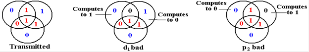
is seen more easily by considering the Venn diagram.
If
d1 is changed in
transmission, the parity bits p1
and p2 will compute to
bad values.
If
d2 is changed in transmission,
the parity bits p1 and p3 will compute to bad
values.
If
d3 is changed in
transmission, the parity bits p2
and p3 will compute to
bad values.
If
d4 is changed in
transmission, the parity bits p1,
p2, and p3 will all compute to bad
values.
Note
that any error in transmitting a single data bit will cause two or more parity
bits to
compute with bad values. If a single
parity bit computes as bad, the logical conclusion is
that the individual parity bit was corrupted in transmission.
The
following diagram illustrates two single–bit errors in transmission.
The
algorithm for identifying and correcting errors based on the computation of the
parity bits
p1, p2, and p3
and comparison with the received values is shown in the table below.
|
p1
|
p2
|
p3
|
Action
|
|
Good
|
Good
|
Good
|
None
required. No single–bit error in
transmission.
|
|
Bad
|
Good
|
Good
|
p1 is bad. Data bits are good. Ignore the parity.
|
|
Good
|
Bad
|
Good
|
p2 is bad. Data bits are good. Ignore the parity.
|
|
Good
|
Good
|
Bad
|
p3 is bad. Data bits are good. Ignore the parity.
|
|
Bad
|
Bad
|
Good
|
d1 is bad. Flip its value.
|
|
Bad
|
Good
|
Bad
|
d2 is bad. Flip its value.
|
|
Good
|
Bad
|
Bad
|
d3 is bad. Flip its value.
|
|
Bad
|
Bad
|
Bad
|
d4 is bad. Flip its value.
|
Consider now
what happens when there are two bit errors in the transmission.
The figure below illustrates three of the possibilities.
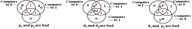
In
the figure at left,p1 and
p2 are bad. This leads to the conclusion that there has
been a single
bit error in d1, whereas
that bit is good and the two parity bits have been corrupted. In the
situation in the middle, only the single parity bit p3 seems to be bad, whereas it is two of the data
bits, d3 and d4, that have been
corrupted. In the situation at right,
one data bit, d1, and one
parity
bit, p3, are
corrupted. None of the three parity bits
compute correctly, leading to the improper
correction of data bit d4.
The
main problem is that the (7, 4)–code will misidentify a double–bit error as a
specific
single–bit error and apply a correction that further corrupts the transmission. The question is
that of how to distinguish when to apply the correction indicated in the above
table and when to
declare an uncorrectable double–bit error.
The answer is found in the parity
of the 7–bit code.
Any single–bit error in the transmitted 7 bits will change the parity, while
any double–bit error
will preserve the parity. The answer is
to declare for either even or odd parity, and append an
appropriate single parity bit to the (7, 4)–code to get an (8, 4)–code. The corrections above are
applied only in the case that the overall parity computes incorrectly.
The
final question on the (7, 4) Hamming code relates to the strange placement of
the
bits to be transmitted. The four data
bits d1, d2, d3, and d4,
and the three parity bits
p1, p2, and p3
are not placed in obvious positions in the transmission sequence. Here is a
table showing the positioning of these bits.
What is the rationale behind this scheme?
|
Bit
|
7
|
6
|
5
|
4
|
3
|
2
|
1
|
|
Value
|
d4
|
d3
|
d2
|
p3
|
d1
|
p2
|
p1
|
The rationale
behind these bit placements can be seen when we consider the table above
containing the corrective actions required.
We consider only the parity bits (bits 1, 2, 4) and
restrict our attention to two–bit and three–bit errors.
Bits
1 and 2 are bad p1 and p2 are bad d1 in bit 3 is bad. Note 1 + 2 = 3.
Bits
1 and 4 are bad p1 and p3 are bad d2 in bit 5 is bad. Note 1 + 4 = 5.
Bits
2 and 4 are bad p2 and p3 are bad d3 in bit 6 is bad. Note 2 + 4 = 6.
Bits
1, 2, and 4 are bad p1 , p2 and p3
are bad d4 in bit 7 is bad.
Note 1 + 2 + 4 = 7.
The
obvious conclusion is that this placement leads to more efficient location of
the bad
data bit; hence more efficient correction of the received data.
A
final observation on the bit placement indicates how this coding method may be
extended
to correct more bits. In order to see
the pattern, we give bit numbers in binary.
p1 in bit 001 is
associated with d1, d2, and d4 in bits 011, 101, 111.
p2 in bit 010 is
associated with d1, d3, and d4 in bits 011, 110, 111.
p3 in bit 100 is
associated with d2, d3, and d4 in bits 101, 110, 111.
Bits
associated with p1 are
the ones with the 1 bit set: 001, 011, 101, and 111.
Bits
associated with p2 are
the ones with the 2 bit set: 010, 011, 110, and 111.
Bits
associated with p3 are
the ones with the 4 bit set: 100, 101, 110, and 111.
This
scheme may be extended to any integer number of parity bits. For p parity bits, the
Hamming code calls for 2p – 1 bits, with d = (2p – 1) – p
data bits. The parity bits are
placed at bits numbered with powers of 2.
Consider
p = 4. 2p – 1 = 24
– 1 = 16 – 1 = 15, and d = 15 –4 = 11.
This is a (15, 11)–code.
Parity
bit p1 is associated with
bits 0001, 0011, 0101, 0111,
1001, 1011, 1101, and 1111.
Parity
bit p2 is associated with
bits 0010, 0011, 0110, 0111, 1010, 1011, 1110, and 1111.
Parity
bit p3 is associated with
bits 0100, 0101, 0110, 0111, 1100, 1101, 1110, and 1111.
Parity
bit p4 is associated with
bits 1000, 1001, 1010, 1011, 1100, 1101, 1110, and 1111.
We
who are mathematically inclined might delight in generating entire families of
Hamming codes. However, two is enough.
Cyclic
Redundancy Check
Check
sums are more robust methods for error detection. This method is an example of those
commonly used on blocks of data, also called “frames”. Data being
transmitted are divided into
blocks of some fixed size and a checksum (a computed integer value, usually 16
or 32 bits) is
appended to the frame for transmission. The
receiver computes this number from the packet data
and compares it to the received value.
If the two match, we assume no error.
This method will
reveal the presence of one or more bit errors in a transmission, but will not
locate the error.
The
CRC (Cyclic Redundancy Check) is a method used by IP (the Internet Protocol) for
transmitting data on the global Internet.
This discussion will follow examples from the textbook
by Kurose and Ross [R032].
The CRC is implemented in hardware using shift registers and
the XOR (Exclusive OR) gate.
The truth table for the Boolean function XOR is as follows
|
X
|
Y
|
X
Å Y
|
|
0
|
0
|
0
|
|
0
|
1
|
1
|
|
1
|
0
|
1
|
|
1
|
1
|
0
|
The
manual process of computing the CRC uses something resembling long division,
except
that the XOR replaces subtraction. The
CRC treats any message M as a sequence of bits.
Denote the number of bits in a message by m. For IP messages, this may be a large number,
say m » 12,000. Append to
this message M of length m a check
sum R of length r. The full
frame thus has a length of (m + r) bits.
For IP version 4, r = 32.
Any of the standard CRC algorithms can detect burst errors
in transmission that do not
exceed r bits. For IP version 4, r = 32, so the CRC can detect burst errors (strings of bad bits)
of length less than 33.
The CRC is generated by an (r + 1)–bit pattern,
called the generator. This is denoted by G.
For IP version 4, this has 33 bits. The
CRC theory is based on the study of polynomials of order
r over GF(2), the field of binary
numbers. For this reason, many
discussions focus on G as a
polynomial, though it can be represented as a binary string. This discussion will proceed with
very little more reference to abstract algebra.
For our example, G is the polynomial X3 + 1,
represented as 1001, which stands for
1·X3 + 0·X2 + 0·X1 + 1.
Note that this is a polynomial of order 3, represented by 4 bits.
In simple terms, the CRC for the message is the remainder
from division of the binary number
M·2r by the binary number
G. In binary, a number is multiplied by
2r by appending r zero
bits.
Example: M = 10111
G = 1001 so r = 3, as G has (r + 1) bits.
M·2r
= 10111 000, the message with 3 zeroes appended.
Converted to decimal, M = 23 and M·2r = M·8 = 184. This may be
interesting, but is of
little use as the system is based on binary numbers.
The generator G is required to have the leftmost (most
significant) bit set to 1. Here it is
the
leading 1, the coefficient of X3.
In this, the standard follows the standard way of naming
polynomials. Consider the polynomial 0·X3 + 1·X2 + 0·X1 + 1.
Some might claim it to be
a cubic, but almost everybody would say that it is the quadratic X2
+ 1.
Begin division, remembering to use the XOR function in place
of subtraction.
10111 000 is being divided by 1001.
_____1____
1001
) 10111000
1001
0010
Here the XOR looks just like subtraction. 1001 is smaller than 1011, so write a 1 in
the “quotient” and perform the XOR to continue.
_____10___
1001
) 10111000
1001
101
We “bring down” the 1 bit and note that 1001 is larger than 101, so write a 0 in the
quotient field and bring down another. We
next “bring down” the 0 and continue.
_____101__
1001
) 10111000
1001
1010
1001
11
Note again, that this is an XOR operation, not binary
subtraction. The result of binary
subtraction would be 1, not 11.
We complete the “division”, discard the quotient and keep
the remainder.
_____10101
1001
) 10111000
1001
1010
1001
1100
1001
101
Here R = 101. Note
that the remainder must be represented as a 3–bit number, so that were it
equal to 11, it would be shown as 011.
To see the utility of the CRC, we divide (M·2r + R) by G.
Here M = 10111
M·2r = 10111000
M·2r + R = 10111101.
In the division below, we see that the remainder is 0. This is a necessary and sufficient
condition for the CRC to determine that the message lacks most common errors.
_____10101
1001
) 10111101
1001
1011
1001
1001
1001
000
All of these computations can be done very efficiently in
hardware. Most implementations
use shift registers and exclusive OR gates.
Shift
Registers and the UART
So
what is a shift register and what does it have to do with the UART (Universal Asynchronous
Receiver and Transmitter)? We shall first
describe a common shift register, then show its
application in computing CRC remainders, and finally show how it functions in a
UART.
As
noted in Chapter 6 of this text (as well as that by Rob Williams [R004]), a
register is just a
collection of flip–flops. Data registers
provide temporary storage for collections of bits. In the
memory system, there is a Memory Buffer Register (MBR). Suppose that the CPU writes to the
main memory one byte at a time. The MBR
would then be a collection of eight flip–flops, one
for each bit to be written. The CPU deposits
the byte in the MBR, which then stores the byte
until it can be copied into main memory.
The CPU continues with other processing.
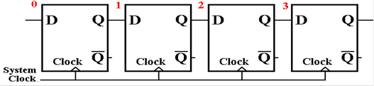
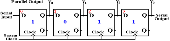
A
data register holding N bits is a collection of N flip–flops that are
essentially independent of
each other. An N–bit shift register is a
collection of flip–flops connected in a special way. The
next figure shows a 4–bit shift register, with the flip–flops numbered in
standard fashion. The
input to flip–flop 0 is some bit source, such as a transmission line. Note that the output of each
flip–flop, except number 3 is fed into the next flip–flop on the clock
pulse. There are a number
of options for the output of the last flip–flop, depending on the use for the
shift register.
The
first step in discussing the shift register is to show what shifts. Then we discuss a
number of standard uses; specifically the CRC computation and the UART.
In
this discussion, we shall make a reasonable assumption about the timing of the
flip–flop.
The output (Q) does not change instantaneously with the input, but only after a
slight delay.
In terms of the clock input to the flip–flop, we assume that the input is
sampled on the rising
edge of the clock pulse and that the output changes some time around the
trailing edge.

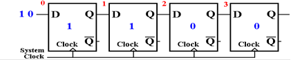
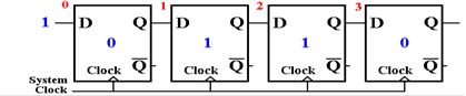
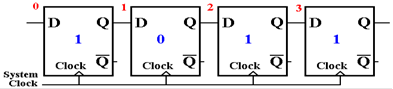
Assume
that the shift register has been initialized to all zeroes, and is given the
input 1011,
LSB first: ‘1’, then ‘1’, then ‘0’, and finally 1. The input is assumed to be synchronized with
the system clock, so that the first ‘1’ is presented just before the rising
edge of the first clock
pulse, and every other bit is presented just before a rising edge.
Here
is the start state of the shift register, just before the first clock pulse.
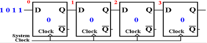
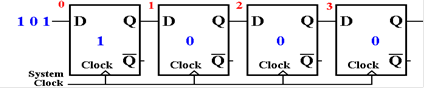
Here
is the state after the first clock pulse.
The LSB has been shifted into the shift register.
After
another clock pulse, another bit has been accepted by the shift register.
After
the third clock pulse, this is the situation.
After
the fourth clock pulse, all of the serial data have been shifted into the shift
register.
Shift
registers are not normally depicted as a collection of flip–flops, but with a
more compact notation. Here is a
standard depiction of a 4–bit shift register.

More
elaborate shift registers will be depicted with parallel input and output lines
(more on that
when we discuss the UART) and control signals for shift direction.
Here
we shall show the use of shift registers and XOR gates to compute the CRC
remainder.
There is a lot of serious mathematics behind this; to be honest, your author
barely understands
this. The goal of this is to display the
simplicity of the circuit.
The
mathematics behind the CRC are based on polynomials with coefficients of 0 or
1.
Here are two polynomials for consideration.
Our
example from earlier X3
+ 1
A realistic polynomial X16
+ X12 + X5 + 1
One
might ask how the realistic, and useful, polynomials are chosen. The design goals are
simple: reduce the probability that a bad block of data will pass muster, and
increase the size
and variety of errors that can be detected successfully. How the choice of polynomial affects
these goals is a topic for very advanced study in modern algebra.
The
design for the CRC detector computing an N–bit CRC remainder, based on an Nth
degree
polynomial, calls for an N–bit shift register.
Thus the teaching example would call for a 3–bit
shift register, while the more realistic example, based on a polynomial of
degree 16, calls for
a 16–bit shift register. Number the
flip–flops in the N–bit shift register from 0 through (N – 1).
The
number of XOR gates used is one less than the number of terms in the
polynomial. For our
teaching example the circuitry would use 1 XOR gate; the realistic example
would use 3.
The
placement of the XOR gates are determined by the powers of X in the
polynomial. Recall
that 1 is X0. For each power
of X, except the highest, an XOR gate is placed just before the
flip–flop with that number. For our
teaching example, this is before flip–flop 0.
For the more
realistic example, this is before flip–flops 0, 5, and 12. Each XOR gate accepts the output of
the most significant flip–flop and the output of the lower flip–flop. The XOR gate feeding
flip–flop 0 accepts the highest–order bit as well as the input line.
Here
is the shift register implementation of the CRC polynomial X3 + 1.
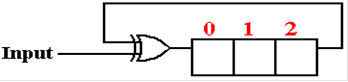
After
the message, with CRC checksum appended, has been processed the 3–bit remainder
is
found in the shift register. A value of
000 indicates the lack of most errors.
We
now show the shift register implementation of the CRC remainder computation for
the polynomial X16 + X12 + X5 + 1. This will call for a 16–bit shift register
with flip–flops
numbered 0 through 15. There will be
three XOR gates, with inputs to flip–flops 0, 5, and 12.
Here is the circuitry. After a
successful CRC check, all 16 flip–flops will be set to 0.

It
would require a lot of mathematics to show that the contents of the above shift
register will
contain the CRC remainder for the message.
Any reader interested in this level of study is
invited to contact the author of these notes.
The UART and Parallel to Serial Conversions
Part
of the job of a UART is to convert between the parallel data format used by the
computer
and the serial data format used by the transmission line. Of course, the UART also handles
clock sampling rates, start bits, and stop bits. The conversion between parallel and serial
data
formats is a natural job for a shift register.
For simplicity, we use 4–bit examples.
A
slight modification of the first example 4–bit shift register will illustrate
the serial to parallel
format conversions. The four bits are
shifted in, and are available as the flip–flop contents after
four clock pulses. The bits are then
transferred out in parallel.
The
reverse process is used for parallel to serial format conversion. The flip–flops are loaded
in parallel, and the serial output provides the bits in sequence as the
register shifts.
The
UART was originally associated with the COM ports on a PC. While these ports may be
in the process of being replaced by the USB port, the idea of data format
conversion persists.
As is the case for much in this chapter, we have covered details that are not
likely to be used by
the average programmer. Your author
believes, however, that a student trained in the study of
computer science should have a passing acquaintance, at least.
The USB
(Universal Serial Bus)
A
modern computer system comprises a CPU, memory, and a number of peripheral
devices, all
connected by busses of some sort. As
computers evolved, so did the bus designs.
However, the
number of bus designs lead to a number of incompatible bus protocols, making it
difficult to
design devices for interface to existing systems. It is worth noting that the success of the
original
PC (by IBM) was in part due to the publication of the bus protocol, allowing
manufacturers of
peripheral devices to design compatible devices.
The
USB design was created by a consortium of manufacturers in the early 1990’s as
a new
standard to handle low speed peripherals.
Pre–release versions of the standard were submitted
for review beginning in November 1994.
Since then there have been 3 official major releases.
|
Version
|
Released
|
Bandwidth
|
|
1.0
|
January
1996
|
1.5
MB/sec
|
|
2.0
|
April
2000
|
60
MB/sec
|
|
3.0
|
November
2008
|
625
MB/sec
|
As of December
2011, most USB devices are designed to version 2.0 of the protocol. It appears
that USB devices are becoming rather popular, displacing many devices designed
for other bus
standards. In your author’s opinion,
this is due to the simplicity of the USB.
The following is
a brief list of USB devices that the author of this textbook uses regularly.
1. A
mouse device that is connected to the PC through a USB port.
2. Three
USB flash drives, now on the smaller size: 2 GB, 4GB, and 16 GB. 64 GB
flash drives are commercially
available and a 256 GB device has been demonstrated.
3. An
external 500 GB disk drive connected to the computer through a USB drive.
This is used for data backup.
4. A
Nikon D100 digital camera, with a USB connection to download digital pictures
to a computer.
5. A
cell phone that uses a USB connection just for power.
6. An
IPOD Nano, that uses a USB connection for power, as well as downloading
pictures and audio files.
The
USB 2.0 standard calls for four wires: two for data transmission, one for power
(+5 V),
and one for ground (0 V). The USB 3.0
standard extends this to ten, including two more
ground lines, a pair of signal transmission lines and a pair of signal
receiving lines. It appears
that the primary mode of operation for USB 3.0 will involve the additional two
pairs of lines,
with the original pair retained for USB 2.0 compatibility.
Questions: What about these pairs of lines for
data? USB 2.0 has one pair, USB 3.0 has
3.
What is a signal
transmission line pair and how does that differ from a
signal receiving
pair?
In
order to answer these questions, we need to give a standard description of the
data line
pair on USB 2.0 and then define the terms used in that description. In standard technical
parlance, the USB 2.0 data lines use half–duplex
differential signaling.
Consider
a pair of communicating nodes. One way
to classify the communication between
them involves the terms simplex, half–duplex, and full–duplex.
A
simplex communication is one way
only. One good example is a standard
radio. There is
a transmitter and a receiver.
In
duplex communication, data can flow
either way between the two nodes. In half–duplex,
communication is one way at a time.
Think of the walkie–talkies of the 1940’s. One could
either transmit or receive, but not both at the same time. The same is true of some amateur
radio sets, because the transmission frequency was the same as the receiving
frequency.
In full–duplex, each side of the
transmission can transmit at the same time.
Modern cell
telephones allow this by using two frequencies: one for transmit and one for
receive.
So,
the USB 2.0 data lines can carry data either way, but only one way at a
time. If either of
the two devices can assert signals on the line (say, a computer and a flash
drive), there must
be some protocol (on a walkie–talkie, one would say “Over” to terminate a
transmission) to
allow the two devices to share the line.
The
data lines form a pair in order to transmit data one way at a time. More precisely, these
lines are a differential pair. We now define that term. It has nothing to do with calculus.
Differential
signaling was developed in response to the problem of noise on a signal
line.
Consider a single transmitter placing a signal on a line. That signal can become so corrupted
with electrical noise from outside sources that it is not useable at the
receiving end. There are
many sources of electrical noise in the environment: electrical motors, arc
welders, etc.
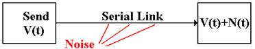
In other words,
the signal received at the destination might not be what was actually transmitted.
The solution to the problem of noise is based on the observation that two links
placed in close
proximity will receive noise signals that are almost identical. To make use of this observation
in order to ameliorate the noise, we use differential
transmitters to send the signals and
differential receivers to
reconstruct the signals.
In differential
transmission, rather than asserting a voltage on a single output line, the
transmitter
asserts two voltages: +V/2 and –V/2. A
+6 volt signal would be asserted as two: +3 volts and –3
volts. A –6 volt signal as –3 volts and
+3 volts, and a 0 volt signal as 0 volts and 0 volts.
Here are the
standard figures for a differential transmitter and differential receiver.
The standard receiver is an analog subtractor, here giving V/2 – (–V/2) = V.
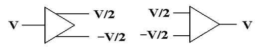
Differential
Transmitter Differential
Receiver
Noise
in a Differential Link
We now assume
that the lines used to transmit the differential signals are physically
close together, so that each line is subject to the same noise signal.
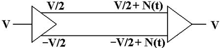
Here the
received signal is the difference of the two voltages input to the differential
receiver.
The value received is ( V/2 +N(t) ) – ( –V/2 + N(t) ) = V, the desired value.
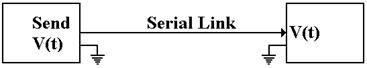
Ground
Offsets in Standard Links
All voltages are
measured relative to a standard value, called “ground”.
Here is the complete version of the simple circuit that we want to implement.
Basically, there
is an assumed second connection between the two devices.
This second connection fixes the zero level for the voltage.
There is no
necessity for the two devices to have the same ground. Suppose that
the ground for the receiver is offset from the ground of the transmitter.
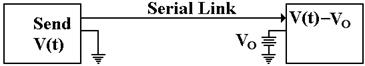
The signal sent
out as +V(t) will be received as V(t) – VO. Here again, the
subtractor in the differential receiver handles this problem.
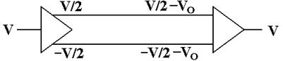
The signal
originates as a given voltage, which can be positive, negative, or 0.
The signal is transmitted as the pair (+V/2, –V/2). Due to the ground offset, the signal is taken
in as
(+V/2 – VO, –V/2 – VO), interpreted as (+V/2 – VO)
– (–V/2 – VO) = +V/2 – VO + V/2 + VO = V.
The differential
link will correct for both ground offset and line noise at the same time.
So far, we have shown that the USB 2.0 standard calls for a
half–duplex differential channel.
The link is one way at a time, and differential signaling is used to reduce the
problem of noise.
What
about the signal transmission lines and signal receiving lines mentioned in the
USB 3.0
standard. Each of these is a pair of
lines that uses half–duplex differential signaling. The two
are paired up in much the same way that many cities facilitate two–way traffic
flow by having
parallel pairs of one–way streets. In
the terminology of the PCI Express bus, these four wires
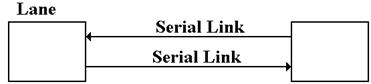
form what is called a lane.
A lane, in PCI Express terminology, is
pair of point–to–point serial links, in other words the lane
is a full–duplex link, able to communicate in two directions
simultaneously. Each of the serial
links in the pair handles one of the two directions. Technically, each of these is a simplex link.
Again, the standard implementation calls for differential signaling, so that
each of these two
serial links would have two wires; a total of four wires for the lane.
Modems
We
close this chapter on a historical note by discussing the modem – modulator/demodulator.
This device allowed computers to communicate over standard telephone
lines. The device has
been made obsolete by the Internet, which provides a more convenient
communication medium.
The
first acoustic modems were developed around 1966 by John Van Geen at Stanford Research
Institute. At that time, Bell Telephone
was a regulated monopoly and legally able to block any
direct connection of non–standard equipment to the telephone line. The modem operated by
converting digital signals into modulated tones for transmission over standard
telephone lines.
It would receive modulated tones and demodulate them into digital signals for processing.
The
biggest restriction on this technology was that the telephone lines were
optimized for
passing human voice; the bandwidth was about 3000 Hz. Even music transmitted over the
telephone sounded bad. Direct digital
signaling was impossible.
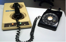 The early modems
were acoustic and connected
The early modems
were acoustic and connected
directly to the handset of a telephone.
The modem
had acoustic insulation around both the mouthpiece
and earpiece of the handset to reduce outside noise.
The
modem had a special speaker that generated the
tones for the telephone mouthpiece, and a special
microphone that detected the tones from the earpiece.
The
brown device is called an “acoustic
coupler”.
Later
versions of the modem allowed direct connection to the telephone lines, without
the
need for an acoustic coupler. Sometimes
the modem connection would allow for a telephone
headset, so that the line could double as a standard land line as well as a
data line.
The
use of modems for distant connection to computing devices seems to have been
replaced
by the global Internet.