Chapter 3 –
The Heritage of the IBM System/360
The IBM System/360 was announced on April 7, 1964. It is considered to be either an early third–generation computer or a hybrid of the second generation and third generation. The goals of this chapter include the following:
1. To
understand the events that lead to the development of the System/360 family
of computers and the context
into which this family must fit.
2. To
understand the motivation for IBM’s creation of a family of computers, with
identical architecture,
spanning a wide range of performance capabilities.
3. To
define the standard five generations of computing technology, relating each
generation to the underlying
circuitry and giving examples of each.
We begin this chapter by addressing the last goal. In order to place the System/360 family correctly, we must study the technologies leading up to it.
The standard division lists five generations, numbered 1 through 5. Here is one such list, taken from the book Computer Structures: Principles and Examples [R04].
1. The
first generation (1945 – 1958) is that of vacuum tubes.
2. The
second generation (1958 – 1966) is that of discrete transistors.
3. The
third generation (1966 – 1972) is that of small-scale and medium-scale
integrated circuits.
4. The
fourth generation (1972 – 1978) is that of large-scale integrated circuits..
5. The
fifth generation (1978 onward) is that of very-large-scale integrated circuits.
This classification scheme is well established and quite useful, but does have its drawbacks. Two that are worth mention are the following.
1. The
term “fifth generation” has yet to be defined in a uniformly accepted way.
For many, we continue to live
with fourth–generation computers and are even now
looking forward to the next
great development that will usher in the fifth generation.
2. This
scheme ignores all work before the introduction of the ENIAC in 1945. To quote
an early architecture book,
much is ignored by this ‘first generation’ label.
“It is a measure of American industry’s generally ahistorical view of things that the title of ‘first generation’ has been allowed to be attached to a collection of machines that were some generations removed from the beginning by any reasonable accounting. Mechanical and electromechanical computers existed prior to electronic ones. Furthermore, they were the functional equivalents of electronic computers and were realized to be such.” [R04, page 35]
The IBM System/360, which is the topic of this textbook, was produced by the International Business Machines Corporation. By 1952, when IBM introduced its first electronic computer, it had accumulated over 50 years experience with tabulating machines and electromechanical computers. In your author’s opinion, this early experience greatly affected the development of all IBM computers; for this reason it is studied.
A Revised Listing of the Generations
We now present the classification scheme to be used in this
textbook. In order to fit the standard
numbering scheme, we follow established practice and begin with “Generation 0”.
Generation 0 (1642 through 1945)
This is the era of purely mechanical calculators and electromechanical
calculators. At this time the term
“computer” was a job title, indicating a human who used a calculating machine.
Generation 1 (1945 through 1958)
This is the era of computers (now defined as machines) based on vacuum tube
technology.
All subsequent generations of computers are based on the transistor, which was developed by Bell Labs in late 1947 and early 1948. It can be claimed that each of the generations that follow represent only a different way to package transistors. Of course, one can also claim that a modern F–18 is just another 1910’s era fighter. Much has changed.
Generation 2 (1958 through 1966)
Bell Labs licensed the technology for transistor fabrication in late 1951
and presented the Transistor Technology Symposium in April 1952. The TX–0, an early experimental computer
based on transistors, it became operational in 1956. IBM’s first transistor–based computer, the
7070, was announced in September 1958.
Generation 3 (1966 through 1972)
This is the era of SSI (Small Scale Integrated) and MSI (Medium Scale
Integrated) circuits. Each of these
technologies allowed the placement of a number of transistors on a single chip
fabricated from silicon, with the wiring between the transistors being achieved
by lines of aluminum actually etched on the chip. There were no large wires on the chip.
SSI corresponded to 100 or fewer electronic components on a chip.
MSI corresponded to between 100 and 3,000 electronic components on a chip.
Generation 4 (1972 – 1978)
This is the era of LSI (Large Scale Integrated) chips, with up to 100,000
components on the chip. Many of the
early Intel processors fall into this generation.
Generation 4 B (1978 and later)
This is the era of VLSI (Very Large Scale Integrated) chips, having more
than 100,000 components on the chip. The
Intel Pentium series belongs here.
This textbook will not refer to any computing technology as “fifth generation”; the term is just too vague and has too many disparate meanings. As a matter of fact, it will not make many references to the fourth generation, as the IBM System/360 family is definitely third generation or earlier.
A Study of Switches
All stored program computers are based on the binary number system,
implemented using some sort of switch that turns voltages on and off. The history of the computer generations is
precisely a history of the devices used as voltage switches. It begins with electromechanical relays and
continues through vacuum tubes and transistors.
Each of the latter two has many uses in analog electronics; the digital
use is a rather specialized modification of the operating regime that causes
each to operate as a switch.
Electronic Relays
Electronic relays are devices that use (often small) voltages to switch other voltages. One example of such a power relay is the horn relay found in all modern automobiles. A small voltage line connects the horn switch on the steering wheel to the relay under the hood. That relay switches a high–current line that activates the horn.
The following figure illustrates the operation of an electromechanical relay. The iron core acts as an electromagnet. When the core is activated, the pivoted iron armature is drawn towards the magnet, raising the lower contact in the relay until it touches the upper contact, thereby completing a circuit. Thus electromechanical relays are switches.
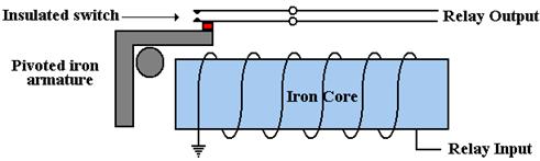
Figure: An Electromechanical Relay
In general, an electromechanical relay is a device that uses an electronic voltage to activate an electromagnet that will pull an electronic switch from one position to another, thus affecting the flow of another voltage; thereby turning the device “off” or “on”. Relays display the essential characteristic of a binary device – two distinct states. Below we see pictures of two recent-vintage electromechanical relays.
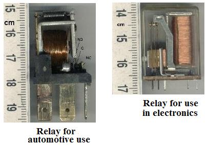
Figure: Two Relays (Source
http://en.wikipedia.org/wiki/Relay)
The primary difference between the two types of relays shown above is the amount of power being switched. The relays for use in general electronics tend to be smaller and encased in plastic housing for protection from the environment, as they do not have to dissipate a large amount of heat. Again, think of an electromechanical relay as an electronically operated switch, with two possible states: ON or OFF.
Power relays, such as the horn relay, function mainly to isolate the high currents associated with the switched apparatus from the device or human initiating the action. One common use is seen in electronic process control, in which the relays isolate the electronics that compute the action from the voltage swings found in the large machines being controlled.
In use for computers, relays are just switches that can be operated electronically. To understand their operation, the student should consider the following simple circuits.
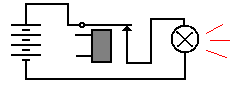
Figure: Relay Is Closed: Light Is
Illuminated
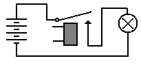
Figure: Relay Is Opened: Light Is Dark.
We may use these simple components to generate the basic Boolean functions, and from these the more complex functions used in a digital computer. The following relay circuit implements the Boolean AND function, which is TRUE if and only if both inputs are TRUE. Here, the light is illuminated if and only if both relays are closed.
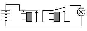
Figure: One Closed and One Open
Computers based on electromagnetic relays played an important part in the early development of computers, but became quickly obsolete when designs using vacuum tubes (considered as purely electronic relays) were introduced in the late 1940’s. These electronic tubes also had two states, but could be switched more quickly as there were no mechanical components to be moved.
Vacuum Tubes
The next step in digital logic was the use of a vacuum tube as a digital switch. As this device was purely electrical, it was much faster than the electromechanical relays that had been used in digital computing machines prior to about 1945. The figure below shows four vacuum tubes from this author’s personal collection. Note that the big one is about 5 inches tall.
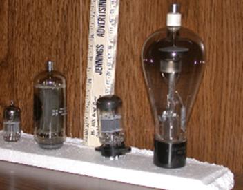
Figure: Four
Vacuum Tubes Mounted in Styrofoam
The big vacuum tube to the right is a diode, which is an element with 3 major components: a filament, a cathode and a grid. This would have been used as a rectifier as a part of a circuit to convert AC (Alternating Current) into DC (Direct Current).
The cathode is the element that is the source of electrons in the tube. When it is heated either directly (as a filament in a light bulb) or indirectly by a separate filament, it will emit electrons, which either are reabsorbed by the cathode or travel to the anode. When the anode is held at a voltage more positive than the cathode, the electrons tend to flow from cathode to anode (and the current is said to flow from anode to cathode – a definition made in the early 19th century before electrons were understood). The anode is the silver “cap” at the top.
One of the smaller tubes is a triode, which has four major components: the above three as well as a controlling grid placed between the cathode and the anode. This serves as a current switch, basically an all–electronic relay. The grid serves as an adjustable barrier to the electrons. When the grid is more positive, more electrons tend to leave the cathode and fly to the anode. When the grid is more negative, the electrons tend to stay at the cathode. By this mechanism, a small voltage change applied to the grid can cause a larger voltage change in the output of the triode; hence it is an amplifier. As a digital device, the grid in the tube either allows a large current flow or almost completely blocks it – “on” or “off”.
Here we should add a note related to analog audio devices, such as high–fidelity and stereo radios and record players. Note the reference to a small voltage change in the input of a tube causing a larger voltage change in the output; this is amplification, and tubes were once used in amplifiers for audio devices. The use of tubes as digital devices is just a special case, making use of the extremes of the range and avoiding the “linear range” of amplification.
We close this section with a picture taken from the IBM 701 computer, a computer from 1952 developed by the IBM Poughkeepsie Laboratory. This was the first IBM computer that relied on vacuum tubes as the basic technology.
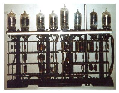
Figure: A Block of Tubes from the IBM 701
Source: [R23]
The reader will note that, though there is no scale on this drawing, the tubes appear rather small, and are probably about one inch in height. The components that resemble small cylinders are resistors; those that resemble pancakes are capacitors.
Another feature of the figure above that is worth note is the fact that the vacuum tubes are grouped together in a single component. The use of such components probably simplified maintenance of the computer; just pull the component, replace it with a functioning copy, and repair the original at leisure.
There are two major difficulties with computers fabricated from vacuum tubes, each of which arises from the difficulty of working with so many vacuum tubes. Suppose a computer that uses 20,000 vacuum tubes; this being only slightly larger than the actual ENIAC.
A vacuum tube requires a hot filament in order to function. In this it is similar to a modern light bulb that emits light due to a heated filament. Suppose that each of our tubes requires only five watts of electricity to keep its filament hot and the tube functioning. The total power requirement for the computer is then 100,000 watts or 100 kilowatts.
We also realize the problem of reliability of such a large collection of tubes. Suppose that each of the tubes has a probability of 99.999% of operating one hour. This can be written as a decimal number as 0.99999 = 1.0 – 10-5. The probability that all 20,000 tubes will be operational for more than an hour can be computed as (1.0 – 10-5)20000, which can be approximated as 1.0 – 20000·10-5 = 1.0 – 0.2 = 0.8. There is an 80% chance the computer will function for one hour and 64% chance for two hours of operation. This is not good.
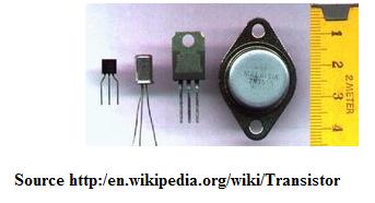
Discrete Transistors
Discrete transistors can be thought of as small triodes with the additional advantages of consuming less power and being less likely to wear out. The reader should note the transistor second from the left in the figure below. It at about one centimeter in size would have been an early replacement for the vacuum tube of about 5 inches (13 centimeters) in size shown on the previous page. One reason for the reduced power consumption is that there is no need for a heated filament to cause the emission of electrons.
When first introduced, the transistor immediately presented an enormous (or should we say small – think size issues) advantage over the vacuum tube. However, there were cost disadvantages, as is noted in this history of the TX–0, a test computer designed around 1951.
“Like the MTC [Memory Test Computer], the TX–0 was designed as a test device. It was designed to test transistor circuitry, to verify that a 256 X 256 (64–K word) core memory could be built … and to serve as a prelude to the construction of a large-scale 36–bit computer. The transistor circuitry being tested featured the new Philco SBT100 surface barrier transistor, costing $80, which greatly simplified transistor circuit design.” [R01, page 127]
That is a cost of $288,000 just for the transistors. Imagine the cost of a 256 MB memory, since each byte of memory would require at least eight, and probably 16, transistors.
Packaging Discrete Transistors
In order to avoid the overwhelming complexity associated with individual wires, components at this time were placed onto discrete cards, with a backplane to connect the cards.
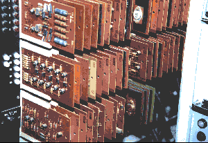
Figure: A Rack
of Circuit Cards from the Z–23 Computer (1961)
The interesting features of these cards are illustrated in the figure below, which is a module called a “Flip Chip”. It was used on a PDP–8 marketed by the Digital Equipment Corporation in the late 1960’s. Note the edge connectors that would plug into a wired backplane. Also note the “silver” traces on the back of the card. These traces served as wires to connect the components that were on the chip. An identical technology, on a very much smaller scale, has been employed by each of the generations of integrated chips.
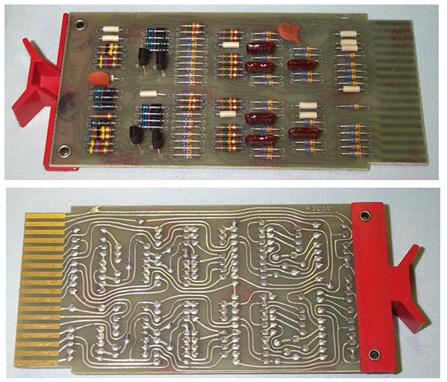
Figure: Front and Back of an R205b
Flip-Chip (Dual Flip-Flop) [R42]
In the above figure, one can easily spot many of the discrete components. The orange pancake-like items are capacitors, the cylindrical devices with colorful stripes are resistors with the color coding indicating their rating and tolerances, the black “hats” in the column second from the left are transistors, and the other items must be something useful. The size of this module is indicated by the orange plastic handle, which is fitted to a human hand.
It was
soon realized that assembly of a large computer from discrete components would
be almost impossible, as fabricating such a large assembly of components
without a single faulty connection or component would be extremely costly. This problem became known as the “tyranny of
numbers”. Two teams independently sought
solutions to this problem. One team at
Texas Instruments was headed by Jack Kilby, an engineer with a background in
ceramic-based silk screen circuit boards and transistor-based hearing
aids. The other team was headed by
research engineer Robert Noyce, a co-founder of Fairchild Semiconductor
Corporation. In 1959, each team applied
for a patent on essentially the same circuitry, Texas Instruments receiving
Integrated Circuits
Integrated circuits are nothing more or less than a very efficient packaging of transistors and other circuit elements. The term “discrete transistors” implied that the circuit was built from transistors connected by wires, all of which could be easily seen and handled by humans.
As noted above, the integrated circuit was independently developed by two teams of engineers in 1959. The advantages of such circuits quickly became obvious and applications in the computer world soon appeared. We list a few of the more obvious advantages.
1. The
integrate circuit solved the “tyranny of numbers” problem mentioned above.
More of the wiring
connections were placed on the chip of the integrated circuit,
which could be automatically
fabricated. This automation of
production lead to
decreased costs and increased
reliability.
2. The
length of wires interconnecting the integrated circuits was decreased, allowing
for much faster
circuitry. In the Cray–1, a supercomputer
build with generation 2
technologies, the longest
wire was 4 feet. Electricity travels on
wires at about two
feet per nanosecond; the
Cray–1 had to allow for 4 nanosecond round trip times.
This limited the maximum
clock frequency to about 200 MHz.
The first integrated circuits were classified as SSI (Small-Scale Integration) in that they contained only a few tens of transistors. The first commercial uses of these circuits were in the Minuteman missile project and the Apollo program. It is generally conceded that the Apollo program motivated the technology, while the Minuteman program forced it into mass production, reducing the costs from about $1,000 per circuit in 1960 to $25 per circuit in 1963. Were such components fabricated today, they would cost less than a penny.
Large Scale and Very
Large Scale Integrated Circuits (from 1972 onward)
As we shall se, the use of SSI (Small Scale Integration) in the early System/360 models yielded an impressive jump in circuit density. We now have a choice: stop here because we have developed the technology to explain the System/360 and System /370, or trace the later evolution of the S/360 family through the S/370 (announced in 1970), the 370/XA (1983), the ESA/370 (1988), the ESA/390 (1990), and the z/Series (announced in 2000).
The major factor driving the development of smaller and more powerful computers was and continues to be the method for manufacture of the chips. This is called “photolithography”, which uses light to transmit a pattern from a photomask to a light–sensitive chemical called “photoresist” that is covering the surface of the chip. This process, along with chemical treatment of the chip surface, results in the deposition of the desired circuits on the chip.
In a very real sense, the development of what might be called “Post Generation 3” circuitry really depended on the development of the automated machinery used to produce those circuits. These machines, together with the special buildings required to house them, are called “Fabs”, or chip fabrication centers. These fabs are also extraordinarily expensive, costing on the order of $ 1 billion dollars. All of this development is in the future for the computers in which we are interested for this course.
We shall limit our thoughts to the first three generations of computer technologies.
It seems that pictures are the best way to illustrate the evolution of the first three generations of computer components. Below, we see a picture of an IBM engineer (they all wore coats and ties at that time) with three generations of components. He is seen sitting in front of the control panel for one of the System/360 models.
The first generation unit (vacuum tubes) is a pluggable module from the IBM 650. Recall that the idea of pluggable modules dates to the ENIAC; the design facilitates maintenance.
The second generation unit (discrete transistors) is a module from the IBM 7090.
The third generation unit is the ACPX module used on the IBM 360/91 (1964). Each chip was created by stacking layers of silicon on a ceramic substrate; it accommodated over twenty transistors. The chips could be packaged together onto a circuit board. Note the pencil pointing to one of the chips on the board. It is likely that this chip has functionality equivalent to the transistorized board on the right or the vacuum tube pluggable unit on the left.
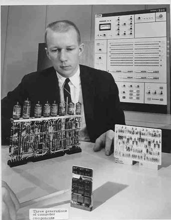
Figure: IBM Engineer with Three Generations
of Components
Magnetic Core Memory
The reader will note that most discussions of the “computer generations” focus on the technology used to implement the CPU (Central Processing Unit). Here, we shall depart from this “CPU–centric view” and discuss early developments in memory technology. We shall begin this section by presenting a number of the early technologies and end it with what your author considers to be the last significant contribution of the first generation – the magnetic core memory. This technology was introduced with the Whirlwind computer, designed and built at MIT in the late 1940’s and early 1950’s.
The
reader will recall that the ENIAC did not have any memory, but just used twenty
10–digit accumulators. For this reason,
it was not a stored program computer, as it had no memory in which to store the
program. A moderately sized memory (say
4 kilobytes) would probably have required 32,768 dual–triode vacuum tubes to
implement. This was not feasible at the
time; it would have cost too much and been far too unreliable.
The EDSAC
Maurice Wilkes of
It should be noted that Dr. Wilkes was primarily interested in creating a machine that he could use to test software development. As a result, the EDSAC was a very conservative design.
Figure: Maurice Wilkes and a Set of 16
mercury delay lines for the EDSAC [R 38]
The
The next step in the development of memory technology was taken at the
Each of the Manchester Baby and the Manchester/Ferranti Mark I computers used a new technology, called the “Williams–Kilburn tube”, as an electrostatic main memory. This device was developed in 1946 by Frederic C. Williams and Tom Kilburn [R43]. The first design could store either 32 or 64 words (the sources disagree on this) of 32 bits each.
The tube was a cathode ray tube in which the binary bits stored would appear as dots on the screen. The next figure shows the tube, along with a typical display; this has 32 words of 40 bits each. The bright dots store a 1 and the dimmer dots store a 0.
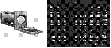
Figure: An
Early Williams–Kilburn tube and its display
Note the extra line of 20 bits at the top.
While the Williams–Kilburn tube sufficed for the storage of the prototype Manchester Baby, it was not large enough for the contemplated Mark I. The design team decided to build a hierarchical memory, using double–density Williams–Kilburn tubes (each storing two pages of thirty–two 40–bit words), backed by a magnetic drum holding 16,384 40–bit words.
The magnetic drum can be seen to hold 512 pages of thirty–two 40–bit words each. The data were transferred between the drum memory and the electrostatic display tube one page at a time, with the revolution speed of the drum set to match the display refresh speed. The team used the experience gained with this early block transfer to design and implement the first virtual memory system on the Atlas computer in the late 1950’s.
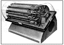
Figure: The IBM
650 Drum Memory
The MIT Whirlwind and Magnetic Core Memory
The MIT Whirlwind was designed as a bit-parallel machine with a 5 MHz
clock. The following quote describes the
effect of changing the design from one using current technology memory modules
with the new core memory modules.
“Initially it [the Whirlwind] was designed using a rank of sixteen Williams tubes, making for a 16-bit parallel memory. However, the Williams tubes were a limitation in terms of operating speed, reliability, and cost.”
“To solve this problem, Jay W. Forrester and others developed magnetic core memories. When the electrostatic memory was replaced with a primitive core memory, the operating speed of the Whirlwind doubled, and the maintenance time on the machine fell from four hours per day to two hours per week, and the mean time between memory failures rose from two hours to two weeks! Core memory technology was crucial in enabling Whirlwind to perform 50,000 operations per second in 1952 and to operate reliably for relative long periods of time” [R11]
The reader should consider the previous paragraph carefully and ask how useful computers would be if we had to spend about half of each working day in maintaining them.
Basically core memory consists of magnetic cores, which are small doughnut-shaped pieces of magnetic material. These can be magnetized in one of two directions: clockwise or counter-clockwise; one orientation corresponding to a logic 0 and the other to a logic 1. Associated with the cores are current carrying conductors used to read and write the memory. The individual cores were strung by hand on the fine insulated wires to form an array. It is a fact that no practical automated core-stringing machine was ever developed; thus core memory was always a bit more costly due to the labor intensity of its construction.
To more clearly illustrate core memory, we include picture from the Sun Microsystems web site. Note the cores of magnetic material with the copper wires interlaced.
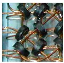
Figure:
Close–Up of a Magnetic Core Memory [R40]
At this point, we leave our discussion of the development of memory technology. While it is true that memory technology advanced considerably in the years following 1960, we have taken our narrative far enough to get us to the IBM System/360 family.
Interlude: Data Storage Technologies In
the 1950’s
We have yet to address methods commonly used by early computers for storage of off–line data; that is data that were not actually in the main memory of the computer. One may validly ask “Why worry about obsolete data storage technologies; we all use disks.” The answer is quite simple, it is the format of these data cards that drove the design of the interactive IBM systems we use even today. We enter code and data as lines on a terminal using a text editor; we should pretend that we are punching cards.
There were two methods in common use at the time. One of the methods employed punched paper tape, with the tape being punched in rows of either five or seven holes. Here are two views of typical punched paper tapes from approximately the 1950’s.
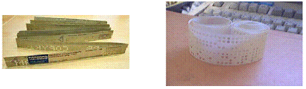
Figure: Punched
Paper Tape – Fanfold and Rolled
While punched paper tape was commonly used for storage on the smaller computers, such as the IBM 1620, punched cards were the preferred medium for the larger computers of the early 1950’s. Even after the wide availability of magnetic disks and magnetic tape drives, the paper card remained a preferred medium for many data applications until quite late. The most common card was the 80–column punch cards, such as seen in the figure below.
Figure:
80–Column Punch Card (Approximately 75% of Full Size)
These cards would store at most eighty characters, so that the maximum data capacity was exactly eighty bytes. The card has twelve rows with the bottom ten being numbered 0 through 9. There are two additional rows (unmarked in this card) on the top.
The data (80 characters maximum) were encoded on the card by punching holds in each column. Most printing punches would print the text corresponding to each column on the top of the card above that column. Anything printed or written on the card (such as the college logo above) would have been ignored; only the holes in the cards were significant.
There are two common coding schemes used by IBM for their punched cards; these are usually identified by the name of the card punch producing them. The IBM 026 card punch, introduced in July 1949, produced cards encoded with BCDIC (Binary Coded Decimal Interchange Code), an extension of Baudot code. The figure below shows the twelve rows (or punching positions) with the codes for each digit, upper case letter, or special character.
There are many features of the IBM 026 that persist into the later IBM 029 and other card punches (if there are any left at the moment). For this reason, we discuss the features here.
Note that the digits 0 through 9 are each encoded with a single punch and that punched hole is placed in the row with the appropriate value. Only the digits have a single punch code; all the other characters have at least two holes punched in their column.
As noted above, there are twelve rows or “punching positions” on this card. The bottom ten rows, labeled rows 0 through 9, are easily seen on the card. The two rows, or punching positions, above these ten rows are called rows 12 and 11; with row 12 nearer the top. Printing card punches would place a line of text at the top of the card, just above punching position 12; as noted above, the card readers would ignore that text.
The easiest way to describe the codes for the upper case letters is by the punching positions used to encode them. Here are a few codes, read from the image above.
A 12
– 1 J 11 – 1
B 12
– 2 K 11 – 2 S 0 – 2
I 12
– 9 R 11 – 9 Z 0 – 9
BCDIC is a 46–character code that includes the 26 uppercase Roman letters, the 10 digits 0-9, and 11 special characters: Ampersand (&), Period (.), Lozenge (◊), Minus sign (-), Dollar sign ($), Asterisk (*), Slash (/), Comma (,), Percent sign (%), Number sign (#), and Commercial At Sign (@).
The reader will note that this code omits all lower case letters and a great number of useful characters. The obvious conclusion is that it predates any high–level programming language, as it lacks coding for the plus sign,”+”, as well as parentheses.
The figure below shows an IBM 026 printing card punch from about the year 1949. The term “printing punch” means that it will write the character above each column encoding that character. Blank cards are fed from the card hopper, one at a time into the punching station. In common usage, after being punched, the cards would move automatically through the reading station (which did nothing) and into the card stacker.
Some of the features shown below, such as the program unit and column indicator, allowed automation of various data entry functions, such as moving to tabbed columns. Programmers rarely used these features, though they could be useful.
Figure: An IBM
026 Printing Card Punch, Circa 1949
The IBM 026 remained in common use until 1964, when the IBM System/360 was introduced. This machine required a new code for its much enlarged character set, EBCDIC (Extended Binary Coded Decimal Interchange Code), and hence a new card punch. EBCDIC was designed as a compatible extension of the older BCDIC; cards produced by the older IBM 026 punches could be interpreted as EBCDIC.
The IBM
029 Printing Card Punch was used to encode characters in EDCDIC on a standard
eighty–column punch card. The format of
the card was retained while the code changed.
Here is an illustration of the punch code produced by the IBM 029; the card
displays each of the 64 characters available for this format. Note again that lower case letters are
missing.
Note that the encodings for the ten digits and twenty–six upper case letters are retained from the BCDIC codes of the IBM 026. This example shows the print representation of each character above the column that encodes it. The IBM 026 also had the ability to print in this area; it is just that the example we noted did not have that printing. Comparison of the picture of the IBM 029 (below) and the IBM 026 (above) show only cosmetic change.
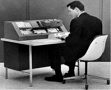
Figure: The IBM
029 Printing Card Punch (1964)
It is worth noting that IBM seriously considered adoption of ASCII as its method for internal storage of character data for the System/360. The American Standard Code for Information Interchange was approved in 1963 and supported by IBM. However the ASCII code set was not compatible with the BCDIC used on a very large installed base of support equipment, such as the IBM 026. Transition to an incompatible character set would have required any adopter of the new IBM System/360 to also purchase or lease an entirely new set of peripheral equipment; this would have been a deterrence to early adoption.
It is a little known fact that the CPU (Central Processing Unit) on an early System/360 implementation included an “ASCII bit” in the PSW (Program Status Word). When set, the S/360 would process characters encoded in ASCII; when cleared the EBCDIC code was used.
It is an interesting study to remark on the design of the EBCDIC scheme and how it was related to the punch card codes used by the IBM 029 card punch. One should be very careful and precise at this moment; the punch card codes were not EBCDIC.
The structure of the EBCDIC, used for internal character storage on the System/360 and later computers, was determined by the requirement for easy translation from punch card codes. The table below gives a comparison of the two coding schemes.
|
Character |
Punch Code |
EBCDIC |
|
‘0’ |
0 |
F0 |
|
‘1’ |
1 |
F1 |
|
‘9’ |
9 |
F9 |
|
‘A’ |
12 – 1 |
C1 |
|
‘B’ |
12 – 2 |
C2 |
|
‘I’ |
12 – 9 |
C9 |
|
‘J’ |
11 – 1 |
D1 |
|
‘K’ |
11 – 2 |
D2 |
|
‘R’ |
11 – 9 |
D9 |
|
‘S’ |
0 – 2 |
E2 |
|
‘T’ |
0 – 8 |
E3 |
|
‘Z’ |
0 – 9 |
E9 |
Remember that the punch card codes represent the card rows punched. Each digit was represented by a punch in a single row; the row number was identical to the value of the digit being encoded.
The
EBCDIC codes are eight–bit binary numbers, almost always represented as two
hexadecimal digits. Some IBM
documentation refers to these digits as:
The first digit is the zone potion,
The second digit is the numeric.
A comparison of the older card punch codes with the EBCDIC shows that its design was intended to facilitate the translation. For digits, the numeric punch row became the numeric part of the EBCDIC representation, and the zone part was set to hexadecimal F. For the alphabetical characters, the second numeric row would become the numeric part and the first punch row would determine the zone portion of the EBCDIC.
This matching with punched card codes explains the “gaps” found in the EBCDIC set. Remember that these codes are given as hexadecimal numbers, so that the code immediately following C9 would be CA (as hexadecimal A is decimal 10). But the code for ‘J’ is not hexadecimal CA, but hexadecimal D1. Also, note that the EBCDIC representation for the letter ‘S’ is not E1 but E2. This is a direct consequence of the design of the punch cards.
Line Printers: The Output Machines
There were two common methods for output of data from early IBM machines: the card punch and the line printer. The card punch was just a computer controlled version of the manual card punches, though with distinctively different configurations. All card punches, manual or automatic, produced cards to be read by the computer’s card reader.
The standard printer of the time was a line printer, meaning that it printed output one line at a time. These devices were just extremely fast and sophisticated typewriters, using an inked ribbon to provide the ink for the printed characters. The ink–jet printer and the laser printer each is a device of a later decade. One should note that only the “high end” laser printers, of the type found in print shops today, are capable of matching the output of a line printer.
The standard printer formats called for output of data into fixed width columns; the maximum width being either 80 columns per line or 132 columns per line. The first picture shows an IBM 716 printer from about 1952. The second show an IBM 1403 printer introduced in 1959. Each appears to be using 132–column width paper.
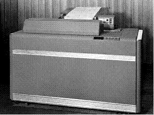
Figure: The IBM
716 Printer
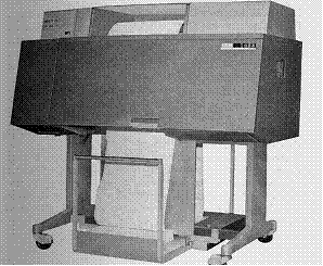
Figure: The IBM 1403 Printer
IBM: Generation 0
We now examine the state of affairs for IBM at the end of the 1940’s. This for IBM was the end of “Generation 0”; that is the time during which electromechanical calculators were phased out and vacuum tube computers were introduced.
The author of this textbook wishes to state that the source for almost all of the material in this section is the IBM history web site (http://www-03.ibm.com/ibm/history/exhibits/).
IBM was
incorporated in the state of
One can argue that the lineage of most of IBM’s product line in the late 1940’s can be traced back to the work of Dr. Herman Hollerith, who first demonstrated his tabulating systems in 1889. This system used punched cards to record the data, and a electromechanical calculator to extract information from the cards.
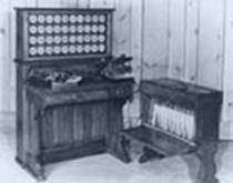 Herman
Hollerith's Tabulating System, shown in the figure to the left, was used in the
U.S. Census of 1890. It reduced a nearly
10–year long process to two and a half years and saved $5 million. The Hollerith, Punch Card Tabulating Machine
used an electric current to sense holes in punched cards and keep a running
total of data. Capitalizing on his success, Hollerith formed the Tabulating
Machine Company in 1896. This was one of the companies that was merged
into the C–T–R Company in 1911.
Herman
Hollerith's Tabulating System, shown in the figure to the left, was used in the
U.S. Census of 1890. It reduced a nearly
10–year long process to two and a half years and saved $5 million. The Hollerith, Punch Card Tabulating Machine
used an electric current to sense holes in punched cards and keep a running
total of data. Capitalizing on his success, Hollerith formed the Tabulating
Machine Company in 1896. This was one of the companies that was merged
into the C–T–R Company in 1911.
We mention the Hollerith Tabulator of 1890 for two reasons. The first is that it represented a significant innovation for the time, one that the descendant company, IBM, could be proud of. The second reason is that it illustrates the design of many of the IBM products of the first half of the twentieth century: accept cards as input, process the data on the cards, and produce information for use by the managers of the businesses using those calculators.
As noted
indirectly above, IBM’s predecessor company, the C–T–R Company, was formed in
1911 by the merger of three companies: Hollerith’s Tabulating Machine Company,
the Computing Scale Company of
 We
now jump ahead to 1933, at which time IBM introduced the Type 285 Numeric
Printing Tabulator. The goal of this
device, as well as its predecessors in the 1920’s, was to reduce the error
caused by the hand copying of numbers from the mechanical counters used in
previous tabulators. By this time, the
data cards had been expanded to 80 columns.
These cards were fed from a tray at the right of the machine, and passed
over the tabulating units.
We
now jump ahead to 1933, at which time IBM introduced the Type 285 Numeric
Printing Tabulator. The goal of this
device, as well as its predecessors in the 1920’s, was to reduce the error
caused by the hand copying of numbers from the mechanical counters used in
previous tabulators. By this time, the
data cards had been expanded to 80 columns.
These cards were fed from a tray at the right of the machine, and passed
over the tabulating units.
Early tabulating machines were essentially single–function calculators. Starting in 1906, tabulators were made more flexible by addition of a wiring panel to let users control their actions to some degree, thus allowing the same machine to be sold into different markets (government, railroad, etc) and used for different purposes. But this also meant that if one machine were to be used for different jobs, it would have to be rewired between each job, often a lengthy process that kept the machine offline for extended periods. In 1928, IBM began to manufacture machines with removable wiring panels, or "plugboards", so programs could be prewired and swapped in and out instantly to change jobs.
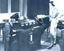
One example of this is the IBM 402 Accounting Machine, introduced in 1948. It was one of the “400 series”, each of which could read standard 80 column cards, accumulate sums, subtotals, and balances, and print reports, all under the control of instructions wired into its control panel. In the figure below, the Type 402 (on the left) is shown attached to a Type 519 Summary Punch (on the right), allowing totals accumulated by the accounting machine to be punched to cards for later use.
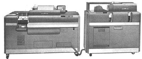
Figure: IBM 402
Attached to an IBM 519
The 402 series, like the 405 before it, used a typebar print mechanism, in which each column (up to 88, depending on model and options) has its own type bar. Long type bars (on the left in the photo below) contain letters and digits; short ones contain only digits (each kind of type bar also includes one or two symbols such as ampersand or asterisk). Type bars shoot up and down independently, positioning the desired character for impact printing.
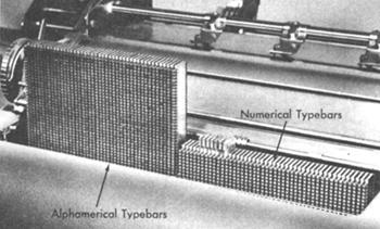
Figure: IBM 402 Tabular Typebar
Here are two views of a plugboard, as used on the IBM Type 402 Accounting Machine.
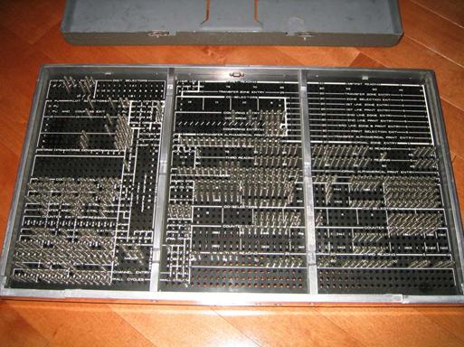
Figure: The
Plugboard Receptacle
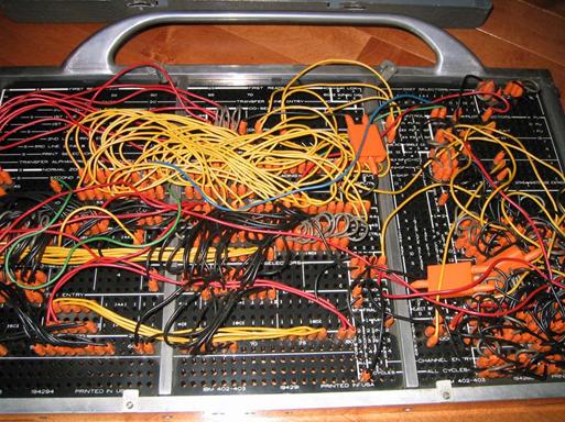
Figure: A Wired
Plugboard
As suggested by the above discussions, most financial computing in the 1930’s and 1940’s revolved around the use of punched cards to store data. The figure below shows a “card shop” from 1950. These 11 men and women are operating an IBM electric accounting machine installation. Seen here (at left) is an IBM 523 gang summary punch, which could process 100 cards a minute and (in the middle) an IBM 82 high-speed sorter, which could process 650 punched cards a minute. This may be seen as an essential part of an IBM shop in the late 1940’s: process financial data and produce results for managers.
Figure: People
with Card Equipment
We close this section of our discussion with a picture of the largest electromechanical calculator ever built, the Harvard Mark I, also known as the IBM Automatic Sequence Controlled Calculator. It was 51 feet long, 8 feet high, and weighed five tons. It was the first fully automatic computer to be completed; once it started it needed no human intervention. It is best seen as an ancestor of the ENIAC and early IBM digital computers.
Figure: The Harvard Mark–I (1944)
The Evolution of the IBM–360
We now return to a discussion of “Big Iron”, a name given informally to the
larger IBM mainframe computers of the time.
Much of this discussion is taken from an article in the IBM Journal of
Research and Development [R46], supplemented by articles from [R1]. We trace the evolution of IBM computers from
the first scientific computer ( the IBM 701, announced in May 1952) through the
early stages of the S/360 (announced in March 1964).
We begin this discussion by considering the situation as of January 1, 1954. At the time, IBM has three models announced and shipping. Two of these were the IBM 701 for scientific computations and the IBM 702 for financial calculations (announced in September 1953),. Each of the designs used Williams–Kilburn tubes for primary memory, and each was implemented using vacuum tubes in the CPU. Neither computer supported both floating–point (scientific) and packed decimal (financial) arithmetic, as the cost to support both would have been excessive. As a result, there were two “lines”: scientific and commercial.
The third model was the IBM 650. It was designed as “a much smaller computer that would be suitable for volume production. From the outset, the emphasis was on reliability and moderate cost”. The IBM 650 was a serial, decimal, stored–program computer with fixed length words each holding ten decimal digits and a sign. Later models could be equipped with the IBM 305 RAMAC (the disk memory discussed and pictured above). When equipped with terminals, the IBM 650 started the shift towards transaction–oriented processing.
The
figure below can be considered as giving the “family tree” of the IBM
System/360.
Note that there are four “lines”: the IBM 650 line, the IBM 701 line, IBM 702
line, and the IBM 7030 (Stretch). The System/360 (so named because it handled
“all 360 degrees of computing”) was an attempt to consolidate these lines and
reduce the multiplicity of distinct systems, each with its distinct maintenance
problems and costs.
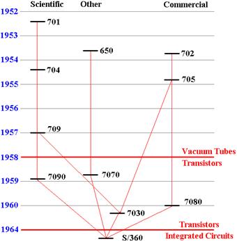
Figure: The IBM
System/360 “Family Tree”
As mentioned above, in the 1950’s IBM supported two product lines: scientific computers (beginning with the IBM 701) and commercial computes (beginning with the IBM 702). Each of these lines was redesigned and considerably improved in 1954.
Generation 1 of the Scientific Line
In the IBM 704 (announced in May 1954), the Williams–Kilburn tube memory was
replaced by magnetic–core memory with up to 32768 36–bit words. This eliminated the most difficult
maintenance problem and allowed users to run larger programs. At the time, theorists had estimated that a
large computer would require only a few thousand words of memory. Even at this time, the practical programmers
wanted more than could be provided.
The IBM 704 also introduced hardware support for floating–point arithmetic, which was omitted from the IBM 701 in an attempt to keep the design “simple and spartan” [R46]. It also added three index registers, which could be used for loops and address modification. As many scientific programs make heavy use of loops over arrays, this was a welcome addition.
The IBM 709 (announced in January 1957) was basically an upgraded IBM 704. The most important new function was then called a “data–synchronizer unit”; it is now called an “I/O Channel”. Each channel was an individual I/O processor that could address and access main memory to store and retrieve data independently of the CPU. The CPU would interact with the I/O Channels by use of special instructions that later were called channel commands.
It was this flexibility, as much as any other factor, that lead to the development of a simple supervisory program called the IOCS (I/O Control System). This attempt to provide support for the task of managing I/O channels and synchronizing their operation with the CPU represents an early step in the evolution of the operating system.
Generation 1 of the Commercial Line
The IBM 702 series differed from the IBM 701 series in many ways, the most
important of which was the provision for variable–length digital
arithmetic. In contrast to the 36–bit
word orientation of the IBM 701 series, this series was oriented towards
alphanumeric arithmetic, with each character being encoded as 6 bits with an
appended parity check bit. Numbers could
have any length from 1 to 511 digits, and were terminated by a “data mark”.
The IBM 705 (announced in October 1954) represented a considerable upgrade to the 702. The most significant change was the provision of magnetic–core memory, removing a considerable nuisance for the maintenance engineers. The size of the memory was at first doubled and then doubled again to 40,000 characters. Later models could be provided with one or more “data–synchronizer units”, allowing buffered I/O independent of the CPU.
Generation 2 of the Product Lines
As noted above, the big change associated with the transition to the second
generation is the use of transistors in the place of vacuum tubes. Compared to an equivalent vacuum tube, a
transistor offers a number of significant advantages: decreased power usage,
decreased cost, smaller size, and significantly increased reliability. These advantages facilitated the design of
increasingly complex circuits of the type required by the then new second
generation.
The IBM 7070 (announced in September 1958 as an upgrade to the IBM 650) was the first transistor based computer marketed by IBM. This introduced the use of interrupt–driven I/O as well as the SPOOL (Simultaneous Peripheral Operation On Line) process for managing shared Input/Output devices.
The IBM 7090 (announced in December 1958) was a transistorized version of the IBM 709 with some additional facilities. The IBM 7080 (announced in January 1960) likewise was a transistorized version of the IBM 705. Each model was less costly to maintain and more reliable than its tube–based predecessor, to the extent that it was judged to be a “qualitatively different kind of machine” [R46].
The IBM 7090 (and later IBM 7094) were modified by researchers at M.I.T. in order to make possible the CTSS (Compatible Time–Sharing System), the first major time–sharing system. Memory was augmented by a second 32768–word memory bank. User programs occupied one bank while the operating system resided in the other. User memory was divided into 128 memory–protected blocks of 256 words, and access was limited by boundary registers.
The IBM 7094 was announced on January 15, 1962. The CTSS effort was begun in 1961, with a version being demonstrated on an IBM 709 in November 1961. CTSS was formally presented in a paper at the Joint Computer Conference in May, 1962. Its design affected later operating systems, including MULTICS and its derivatives, UNIX and MS–DOS.
As a last comment here, the true IBM geek will note the omission of any discussion of the IBM 1401 line. These machines were often used in conjunction with the 7090 or 7094, handling the printing, punching, and card reading chores for the latter. It is just not possible to cover every significant machine.
The IBM 7030 (Stretch)
In late 1954, IBM decided to undertake a very ambitious research project,
with the goal of benefiting from the experience gained in the previous three
project lines. In 1955, it was decided
that the new machine should be at least 100 times as fast as either the IBM 704
or the IBM 705; hence the informal name “Stretch” as it “stretched the
technology”.
In order to achieve these goals, the design of the IBM 7030 required a considerable number of innovations in technology and computer organization; a few are listed here.
1. A
new type of germanium transistor, called “drift transistor” was developed. These
faster transistors allowed
the circuitry in the Stretch to run ten times faster.
2. A new type of core memory was developed; it was 6 times faster than the older core.
3. Memory
was organized into multiple 128K–byte units accessed by low–order
interleaving, so that
successive words were stored in different banks. As a result,
new data could be retrieved
at a rate of one word every 200 nanoseconds, even
though the memory cycle time
was 2.1 microseconds (2,100 nanoseconds).
4. Instruction
lookahead (now called “pipelining”) was introduced. At any point in
time, six instructions were
in some phase of execution in the CPU.
5. New
disk drives, with multiple read/write arms, were developed. The capacity and
transfer rate of these
devices lead to the abandonment of magnetic drums.
6. A
pair of boundary registers were added so as to provide the storage protection
required in a
multiprogramming environment.
It is generally admitted that the Stretch did not meet its design goal of a 100 times increase in the performance of the earlier IBM models. Here is the judgment by IBM from 1981 [R46].
“For a typical 704 program, Stretch fell short of is performance target of one hundred times the 704, perhaps by a factor of two. In applications requiring the larger storage capacity and word length of Stretch, the performance factor probably exceeded one hundred, but comparisons are difficult because such problems were not often tackled on the 704.” [R46]
It seems that production of the IBM 7030 (Stretch) was limited to nine machines, one for Los Alamos National Labs, one (called “Harvest”) for the National Security Agency, and 7 more.
Smaller Integrated
Circuits (Generation 3 – from 1966 to 1972)
In one sense, the evolution of computer components can be said to have stopped in 1958 with the introduction of the transistor; all future developments merely represent the refinement of the transistor design. This statement stretches the truth so far that it hardly even makes this author’s point, which is that packaging technology is extremely important.
What we see in the generations following the introduction of the transistor is an aggressive miniaturization of both the transistors and the traces (wires) used to connect the circuit elements. This allowed the creation of circuit modules with component densities that could hardly have been imagined a decade earlier. Such circuit modules used less power and were much faster than those of the second generation; in electronics smaller is faster. They also lent themselves to automated manufacture, thus increasing component reliability.
The
Control Unit and Emulation
In order to better explain one of the distinctive features of the IBM System/360
family, it is necessary to take a detour and discuss the function of the
control unit in a stored program computer.
Basically, the control unit tells the computer what to do.
All modern stored program computers execute programs that are a sequence of binary machine–language instructions. This sequence of instructions corresponds either to an assembly language program or a program in a higher–level language, such as C++ or Java.
The basic operation of a stored program computer is called “fetch–execute”, with many variants on this name. Each instruction to be executed is fetched from memory and deposited in the Instruction Register, which is a part of the control unit. The control unit interprets this machine instruction and issues the signals that cause the computer to execute it.
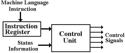
Figure:
Schematic of the Control Unit
There are two ways in which a control unit may be organized. The most efficient way is to build the unit entirely from basic logic gates. For a moderately–sized instruction set with the standard features expected, this leads to a very complex circuit that is difficult to test.
In 1951, Maurice V. Wilkes (designer of the EDSAC, see above) suggested an organization for the control unit that was simpler, more flexible, and much easier to test and validate. This was called a “microprogrammed control unit”. The basic idea was that control signals can be generated by reading words from a micromemory and placing each in an output buffer.
In this design, the control unit interprets the machine language instruction and branches to a section of the micromemory that contains the microcode needed to emit the proper control signals. The entire contents of the micromemory, representing the sequence of control signals for all of the machine language instructions is called the microprogram. All we need to know is that the microprogram is stored in a ROM (Read Only Memory) unit.
While microprogramming was sporadically investigated in the 1950’s, it was not until about 1960 that memory technology had matured sufficiently to allow commercial fabrication of a micromemory with sufficient speed and reliability to be competitive. When IBM selected the technology for the control units of some of the System/360 line, its primary goal was the creation of a unit that was easily tested. Then they got a bonus; they realized that adding the appropriate blocks of microcode could make a S/360 computer execute machine code for either the IBM 1401 or IBM 7094 with no modification. This greatly facilitated upgrading from those machines and significantly contributed to the popularity of the S/360 family.
The IBM System/360
As noted above, the IBM chose to replace a number of very successful, but
incompatible, computer lines with a single computer family, the System/360. The goal, according to an IBM history web
site [R48] was to “provide an expandable system that would serve every data
processing need”. The initial
announcement on April 7, 1964 included Models 30, 40, 50, 60, 62, and 70
[R49]. The first three began shipping in
mid–1965, and the last three were replaced by the Model 65 (shipped in November
1965) and Model 75 (January 1966).
The introduction of the
System/360 is also the introduction of the term “architecture”
as applied to computers. The following
quotes are taken from one of the first papers
describing the System/360 architecture [R46].
“The
term architecture
is used here to describe the attributes of a system as seen by
the programmer,, i.e., the conceptual structure and functional behavior, as
distinct
from the organization of the data flow and controls, the logical design,
and the physical implementation.”
“In the
last few years, many computer architects have realized, usually implicitly,
that logical structure (as seen by the programmer) and physical structure (as
seen
by the engineer) are quite different.
Thus, each may see registers, counters, etc.,
that to the other are not at all real entities.
This was not so in the computers of the
1950’s. The explicit recognition of the
duality of the structure opened the way
for the compatibility within System/360.”
To see the difference, consider the sixteen general–purpose registers (R0 – R15) in the System/360 architecture. All models implement these registers and use them in exactly the same way; this is a requirement of the architecture. As a matter of implementation, a few of the lower end S/360 family actually used dedicated core memory for the registers, while the higher end models used solid state circuitry on the CPU board.
The difference between organization and implementation is seen by considering the two computer pairs: the 709 and 7090, and the 705 and 7080. The IBM 7090 had the same organization (hence the same architecture) as the IBM 709; the implementation was different. The IBM 709 used vacuum tubes; the IBM 7090 replaced these with transistors.
The requirement for the
System/360 design is that all models in that series would be
“strictly program compatible, upward and downward, at the program bit
level”. [R46]
“Here it
[strictly program compatible] means that a valid program, whose logic will
not depend implicitly upon time of execution and which runs upon configuration
A,
will also run on configuration B if the latter includes as least the required
storage, at
least the required I/O devices, and at least the required optional features.”
“Compatibility
would ensure that the user’s expanding needs be easily accommodated
by any model. Compatibility would also
ensure maximum utility of programming
support prepared by the manufacturer, maximum sharing of programs generated by
the user, ability to use small systems to back up large ones, and exceptional
freedom in configuring systems for particular applications.”
Additional design goals for the System/360 include the following.
1. The System/360 was intended to replace two mutually incompatible
product
lines in existence at the
time.
a) The scientific series (701, 704, 7090, and
7094) that supported floating
point arithmetic,
but not decimal arithmetic.
b) The commercial series (702, 705, and 7080)
that supported decimal
arithmetic, but
not floating point arithmetic.
2. The System/360 should have a
“compatibility mode” that would allow it
to run unmodified machine
code from the IBM 1401 – at the time a very
popular business machine
with a large installed base.
This
was possible due to the use of a microprogrammed control unit. If you
want to run native S/360
code, access that part of the microprogram.
If you
want to run IBM 1401 code,
just switch to the microprogram for that machine.
3. The Input/Output Control Program should be
designed to allow execution by
the CPU itself (on smaller
machines) or execution by separate I/O Channels
on the larger machines.
4. The system must allow for autonomous
operation with very little intervention by
a human operator. Ideally this would be limited to mounting and
dismounting
magnetic tapes, feeding
punch cards into the reader, and delivering output.
5. The system must support some sort of
extended precision floating point
arithmetic, with more
precision than the 36–bit system then in use.
The design goal for the series is illustrated by the following scenario. It should be noted that this goal of upward compatibility has persisted to the present day, in which there seem to be at least fifty models of the z/10, all compatible with each other and differing only in performance (number of transactions per second) and cost. Here is the scenario.
1. You have a small company. It needs only a small computer to handle its
computing needs. You lease an IBM System 360/30. You use it in emulation
mode to run your IBM 1401
programs unmodified.
2. Your company grows. You need a bigger computer. Lease a 360/50.
3. You hit the “big time”. Turn in the 360/50 and lease a 360/91.
You never need to rewrite
or recompile your existing programs.
You can still run your IBM
1401 programs without modification.
The System/360 Evolves into the System 370
In June 1970, IBM announced the S/370 as a successor to the System/360. This introduced another design feature of the evolving series; each model would be backwardly compatible with the previous models in that it would run code assembled on the earlier models. Thus, the S/370 would run S/360 code unaltered, and later models would run both S/360 and S/370 code unaltered. It is this fact that we rely on when we are running S/370 assembler code on a modern z/10 Enterprise Server, which was introduced in 2008.
The S/370 underwent a major upgrade to the S/370–XA (S/370 extended architecture) in early 1983. At this time the address space was extended from 24 bits to 31 bits, allowing the CPU to address two gigabytes of memory (1 GB = 230 bytes) rather than just 16 MB (224 bytes).
While the IBM mainframe architecture has evolved further since the introduction of the S/370, it is here that we stop our overview. The primary reason for this is that this course has been designed to teach System/370 Assembler Language, focusing on the basics of that language and avoiding the extensions of the language introduced with the later models.
The Mainframe Evolves: The z10
While this textbook and the course based on it will focus on the state of mainframe assembler writing as of about 1979 (the date at which the textbook we previously used was published), it is important to know where IBM has elected to take this architecture. The present state of the design is reflected in the z/Series, first introduced in the year 2000.
The major design goal of the z/Series is reflected in its name, in which the “z” stands for “Zero Down–Time”. The mainframe has evolved into a highly reliable transaction server for very high transaction volumes. A typical transaction takes place every time a credit card is used for a purchase. The credit card reader at the merchant location contacts a central server, which might be a z10, and the transaction is recorded for billing later. In such a high–volume business, loss of the central server for as much as an hour could result in the loss of millions of dollars in profits to a company. It is this model for which IBM designed the mainframe.
We end this chapter by noting that some at IBM prefer to discontinue the use of the term “mainframe”, considering it to be obsolete. In this thought, the term would refer to an early S/360 or S/370, and not to the modern z/Series systems which are both more powerful and much smaller in physical size. The preferred term would be “Enterprise Server”. The only difficulty is that the customers prefer the term “mainframe”, so it stays.