Fetch-Execute Cycle
As we shall see, the fetch-execute
cycle forms the basis for operation of a stored-program computer. The CPU fetches each instruction from the
memory unit, then executes that instruction, and fetches the next
instruction. An exception to the “fetch
next instruction” rule comes when the equivalent of a Jump or Go To instruction
is executed, in which case the instruction at the indicated address is fetched
and executed.
Registers vs. Memory
Registers and memory are similar in that both store data. The difference between the two is somewhat an
artifact of the history of computation, which has become solidified in all
current architectures. The basic
difference between devices used as registers and devices used for memory
storage is that registers are faster and more expensive.
In modern computers, the CPU is
usually implemented on a single chip.
Within this context, the difference between registers and memory is that
the registers are on the CPU chip while most memory is on a different chip. As a result of this, the registers are not
addressed in the same way as memory – memory is accessed through an address in
the MAR (more on this later), while registers are directly addressed. Admittedly the introduction of cache memory has somewhat blurred the
difference between registers and memory – but the addressing mechanism remains
the primary difference.
The CPU contains two types of
registers, called special purpose
registers and general purpose
registers. The general purpose
registers contain data used in computations and can be accessed directly by the
computer program. The special purpose
registers are used by the control unit to hold temporary results, access
memory, and sequence the program execution.
Normally, with one now-obsolete exception, these registers cannot be
accessed by the program.
The program status register (PSR), also called “program status word (PSW)”, is one of the special purpose
registers found on most computers. The
PSR contains a number of bits to reflect the state of the CPU as well as the
result of the most recent computation.
Some of the common bits are
C the carry-out
from the last arithmetic computation
V Set to 1 if the last arithmetic operation resulted in an overflow
N Set to 1 if the last arithmetic operation resulted in a negative number
Z Set to 1 if the last arithmetic operation resulted in a zero
I Interrupts enabled
(Interrupts are discussed later)
The CPU (Central Processing
Unit)
The CPU is that part of the computer that “does the work”. It fetches and executes the machine language
that represents the program under execution.
It responds to the interrupts (defined later) that usually signal
Input/Output events, but which can signal issues with the memory as well as
exceptions in the program execution. As
indicated above, the CPU has three major components:
1) the ALU
2) the Control Unit
3) the register set
a) the general purpose register file
b) a number of special purpose registers
used by the control unit.
The ALU (Arithmetic–Logic Unit)
This unit is the part of the CPU that carries out the arithmetic and
logical operations of the CPU, hence its name.
The ALU acts in response to control signals issued by the Control
Unit. Quite often there is an attached
floating–point unit that handles all real–number arithmetic, so it is not
completely accurate to say that the ALU handles all arithmetic.
The Control Unit
This unit interprets the machine language representing the computer program
under execution and issues the control signals that are necessary to achieve
the effect that should be associated with the program. This is often the most complex part of the
CPU.
Structure of a Typical Bus
A typical computer contains a number of bus structures. We have already mentioned the system bus and
a bus internal to the CPU. Some computer
designs include high-speed point-to-point busses, used for such tasks as
communication to the graphics card. In
this section, we consider the structure of the system bus. The system bus
is a multi-point bus that allows
communication between a number of devices that are attached to the bus. There are two classes of devices that can be
connected to the bus.
Master Device a device that can initiate action on the bus.
The
CPU is always a bus master.
Slave Device a device that responds to requests by a bus master.
Memory
is an excellent example of a slave device.
Devices
connected to a bus are often accessed by address. System memory is a primary example of an
addressable device; in a byte-addressable
machine (more later on this), memory can be considered as an array of
bytes, accessed in the same way as an array as seen in a typical programming
language. I/O devices are often accessed
by address; it is up to the operating system to know the address used to access
each such device.
Memory Organization and Addressing
We now give
an overview of RAM – Random Access Memory. This is the memory called “primary memory” or “core
memory”. The term “core” is a reference
to an earlier memory technology in which magnetic cores were used for the
computer’s memory. This discussion will
pull material from a number of chapters in the textbook.
Primary
computer memory is best considered as an array of addressable units. Such a unit is the smallest unit of memory
that can have an independent address. In
a byte–addressable memory unit, each byte (8 bits) has an independent address,
although the computer often groups the bytes into larger units (words, long
words, etc.) and retrieves that group.
Most modern computers manipulate integers as 32–bit (4–byte) entities, but
64–bit integers are becoming common.
Many modern designs retrieve multiple bytes at a time.
In this
author’s opinion, byte addressing in computers became important as the result
of the use of 8-bit character codes.
Many applications involve the movement of large numbers of characters
(coded as ASCII or EBCDIC) and thus profit from the ability to address single
characters. Some computers, such as the
CDC-6400, CDC-7600, and all Cray models, use word addressing. This is a result of a design decision made
when considering the main goal of such computers – large computations involving
floating point numbers. The word size in
these computers is 60 bits (why not 64? – I don’t know), yielding good
precision for numeric simulations such as fluid flow and weather prediction.
Memory as a Linear Array
Consider a byte-addressable memory with N bytes of memory. As stated above, such a memory can be
considered to be the logical equivalent of a C++ array, declared as
byte memory [N]
; // Address ranges from 0 through (N –
1)
The
computer on which these notes were written has 384 MB of main memory, now only
an average size but once unimaginably large.
384 MB = 384·220
bytes and the memory is byte-addressable, so N = 384·1048576 =
402,653,184. Quite often the memory size
will either be a power of two or the sum of two powers of two; 384 MB = (256 +
128)·220
= 228 + 227.
Early
versions of the IBM S/360 provided addressability of up to 224 =
16,777,216 bytes of memory, or 4,194,304 32–bit words. All addresses in the S/360 series are byte
addresses.
The term “random access” used when discussing
computer memory implies that memory can be accessed at random with no
performance penalty. While this may not
be exactly true in these days of virtual memory, the key idea is simple – that
the time to access an item in memory does not depend on the address given. In this regard, it is similar to an array in
which the time to access an entry does not depend on the index. A magnetic tape is a typical sequential access device – in order to
get to an entry one must read over all pervious entries.
There are
two major types of random-access computer memory. These are:
RAM Read-Write Memory
ROM Read-Only Memory
The usage of the term “RAM” for
the type of random access memory that might well be called “RWM” has a long
history and will be continued in this course.
The basic reason is probably that the terms “RAM” and “ROM” can easily
be pronounced; try pronouncing “RWM”.
Keep in mind that both RAM and ROM are random access memory.
Of course, there is no such
thing as a pure Read–Only memory; at some time it must be possible to put data
in the memory by writing to it, otherwise there will be no data in the memory
to be read. The term “Read-Only” usually
refers to the method for access by the CPU.
All variants of ROM share the feature that their contents cannot be
changed by normal CPU write operations.
All variants of RAM (really Read-Write Memory) share the feature that
their contents can be changed by normal CPU write operations. Some forms of ROM have their contents set at
time of manufacture, other types called PROM
(Programmable ROM), can have contents changed by special devices called PROM
Programmers.
The Idea of Address Space
We now must
distinguish between the idea of address space and physical memory. The address space defines the range of
addresses (indices into the memory array) that can be generated. The size of the physical memory is usually
somewhat smaller, this may be by design (see the discussion of memory-mapped
I/O below) or just by accident.
The memory
address is specified by a binary number placed in the Memory Address Register
(MAR). The number of bits in the MAR
determines the range of addresses that can be generated. N address lines can be used to specify 2N
distinct addresses, numbered 0 through 2N – 1. This is called the address space of
the computer. The early IBM S/360 had a
24–bit MAR, corresponding to an address space of 0 through 224 – 1,
or 0 through 4,194,303.
For
example, we show some MAR sizes.
Computer
|
MAR bits
|
Address Range
|
|
PDP-11/20
|
16
|
0 to 65,535
|
|
Intel 8086
|
20
|
0 to
1,048,575
|
|
IBM 360
|
24
|
0 to 4,194,303
|
|
S/370–XA
|
31
|
0 to 2,147,483,647
|
|
Pentium
|
32
|
0 to 4,294,967,295
|
|
z/Series
|
64
|
A very big number.
|
The
PDP-11/20 was an elegant small machine made by the now defunct Digital
Equipment Corporation. As soon as it was
built, people realized that its address range was too small.
In general,
the address space is much larger than the physical memory available. For example, my personal computer has an
address space of 232 (as do all Pentiums), but only 384MB = 228
+ 227 bytes. Until recently
the 32–bit address space would have been much larger than any possible amount
of physical memory. At present one can
go to a number of companies and order a computer with a fully populated address
space; i.e., 4 GB of physical memory.
Most high-end personal computers are shipped with 1GB of memory.
Word Addresses in a
Byte-Addressable Machine
Most computers today,
including all of those in the IBM S/360 series, have memories that are byte-addressable;
thus each byte in the memory has a unique address that can be used to address
it. Under this addressing scheme, a word
corresponds to a number of addresses.
A 16-bit word at address Z contains
bytes at addresses Z and Z + 1.
A 32-bit word at address Z contains
bytes at addresses Z, Z + 1, Z + 2, and Z + 3.
In many
computers with byte addressing, there are constraints on word addresses.
A 16-bit word must have an even
address
A 32-bit word must have an address
that is a multiple of 4.
This is
true of the IBM S/360 series in which 16–bit words are called “halfwords”,
32–bit words are called “words”, and 64–bit words are called “double words”. A halfword must have an even address, a word
must have an address that is a multiple of 4 and a double word (64 bits) an
address that is a multiple of 8.
Even in computers that do not
enforce this requirement, it is a good idea to observe these word
boundaries. Most compilers will do so
automatically.
Suppose a
byte-addressable computer with a 24–bit address space. The highest byte address is 224 –
1. From this fact and the address
allocation to multi-byte words, we conclude
the highest address for a 16-bit
word is (224 – 2), and
the highest address for a 32-bit
word is (224 – 4), because the 32–bit word addressed at (224 – 4) comprises bytes
at addresses (224 – 4), (224 – 3), (224 – 2),
and (224 – 1).
Byte Addressing vs. Word Addressing
We have noted above that N address lines can be used
to specify 2N distinct addresses, numbered 0 through 2N –
1. We now ask about the size of the
addressable items. As a simple example,
consider a computer with a 24–bit address space. The machine would have 16,777,216 (16M)
addressable entities. In a byte–addressable
machine, such as the
IBM S/360, this would correspond to:
16 M Bytes 16,777,216 bytes, or
8 M halfwords 8,388,608 16-bit
halfwords, or
4 M words 4,194,304 32–bit
fullwords.
The
advantages of byte-addressability are clear when we consider applications that
process data one byte at a time. Access
of a single byte in a byte-addressable system requires only the issuing of a
single address. In a 16–bit word
addressable system, it is necessary first to compute the address of the word
containing the byte, fetch that word, and then extract the byte from the two–byte
word. Although the processes for byte
extraction are well understood, they are less efficient than directly accessing
the byte. For this reason, many modern
machines are byte addressable.
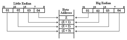
Big–Endian and Little–Endian
The reference here is to a story in Gulliver’s
Travels written by Jonathan Swift in which two groups went to war over
which end of a boiled egg should be broken – the big end or the little
end. The student should be aware that Swift
did not write pretty stories for children but focused on biting satire; his
work A Modest Proposal is an excellent example.
Consider
the 32-bit number represented by the eight–digit hexadecimal number 0x01020304,
stored at location Z in memory. In all
byte–addressable memory locations, this number will be stored in the four
consecutive addresses Z, (Z + 1), (Z + 2), and (Z + 3). The difference between big-endian and
little-endian addresses is where each of the four bytes is stored.
In
our example 0x01 represents
bits 31 – 24,
0x02
represents bits 23 – 16,
0x03
represents bits 15 – 8, and
0x04
represents bits 7 – 0.
As a 32-bit
signed integer, the number represents 01·(256)3 + 02·(256)2
+ 03·(256)
+ 04
or 0·167
+ 1·166
+ 0·165
+ 2·164
+ 0·163
+ 3·162
+ 0·161
+ 4·160,
which evaluates to
1·16777216
+ 2·65536
+ 3·256
+ 4·1
= 16777216 + 131072 + 768 + 4 = 16909060.
Note that the number can be
viewed as having a “big end” and a “little end”, as in the next figure.

The “big
end” contains the most significant digits of the number and the “little end”
contains the least significant digits of the number. We now consider how these bytes are stored in
a byte-addressable memory. Recall that
each byte, comprising two hexadecimal digits, has a unique address in a
byte-addressable memory, and that a 32-bit (four-byte) entry at address Z
occupies the bytes at addresses Z, (Z + 1), (Z + 2), and (Z + 3). The hexadecimal values stored in these four
byte addresses are shown below.
Address Big-Endian Little-Endian
Z 01 04
Z +
1 02 03
Z +
2 03 02
Z +
3 04 01
The figure
below shows a graphical way to view these two options for ordering the bytes
copied from a register into memory. We
suppose a 32-bit register with bits numbered from 31 through 0. Which end is placed first in the memory – at
address Z? For big-endian, the “big end” or most significant byte is first
written. For little-endian, the “little
end” or least significant byte is written first.
Just to be
complete, consider the 16-bit number represented by the four hex digits 0A0B,
with decimal value 10·256 + 11 = 2571. Suppose that the 16-bit word is at
location W; i.e., its bytes are at locations W and (W + 1). The most significant byte is 0x0A and the
least significant byte is 0x0B. The
values in the two addresses are shown below.
Address Big-Endian Little-Endian
W 0A 0B
W + 1 0B 0A
Here we
should note that the IBM S/360 is a “Big Endean” machine.
As an
example of a typical problem, let’s examine the following memory map, with byte
addresses centered on address W. Note
the contents are listed as hexadecimal numbers.
Each byte is an 8-bit entry, so that it can store unsigned numbers between
0 and 255, inclusive. These are written
in hexadecimal as 0x00 through 0xFF inclusive.
|
Address
|
(W – 2)
|
(W – 1)
|
W
|
(W + 1)
|
(W + 2)
|
(W + 3)
|
(W + 4)
|
|
Contents
|
0B
|
AD
|
12
|
AB
|
34
|
CD
|
EF
|
We first
ask what 32-bit integers are stored at address W. Recalling that the value of the number stored
depends on whether the format is big-endian or little-endian, we draw the
memory map in a form that is more useful.
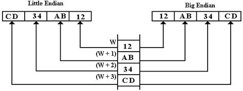
This figure
should illustrate one obvious point: the entries (W – 2), (W – 1), and (W + 4)
are “red herrings”, data that have nothing to do with the problem at hand. We now consider the conversion of the number
in big-endian format. As a decimal
number, this evaluates to
1·167 + 2·166
+ A·165
+ B·164
+ 3·163
+ 4·162
+ C·161
+ D, or
1·167 + 2·166
+ 10·165
+ 11·164
+ 3·163
+ 4·162
+ 12·161
+ 13, or
1·268435456 + 2·16777216 + 10·1048576 + 11·65536 + 3·4096 + 4·256 + 12·16 + 13, or
268435456 + 33554432 +
10485760 + 720896 + 12288 + 1024 + 192 + 13, or
313210061.
The
evaluation of the number as a little–endian quantity is complicated by the fact
that the number is negative. In order to maintain continuity, we convert to
binary (recalling that
A = 1010, B = 1011, C = 1100, and D = 1101) and take the two’s-complement.
Hexadecimal CD 34 AB 12
Binary 11001101 00110100 10101011 00010010
One’s Comp 00110010 11001011 01010100 11101101
Two’s Comp 00110010 11001011 01010100 11101110
Hexadecimal 32 AB 54 EE
Converting
this to decimal, we have the following
3·167 + 2·166
+ A·165
+ B·164
+ 5·163
+ 4·162
+ E·161
+ E, or
3·167 + 2·166
+ 10·165
+ 11·164
+ 5·163
+ 4·162
+ 14·161
+ 14, or
3·268435456 + 2·16777216 + 10·1048576 + 11·65536 + 5·4096 + 4·256 + 14·16 + 14, or
805306368
+ 33554432 + 10485760 + 720896 + 20480 + 1024 + 224 + 14, or
850089198
The number
represented in little-endian form is – 850,089,198.
We now
consider the next question: what 16-bit integer is stored at address W? We begin our answer by producing the drawing
for the 16-bit big-endian and little-endian numbers.
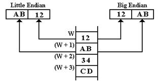
The
evaluation of the number as a 16-bit big-endian number is again the simpler
choice. The decimal value is 1·163
+ 2·162
+ 10·16
+ 11 = 4096 + 512 + 160 + 11 = 4779.
The
evaluation of the number as a little–endian quantity is complicated by the fact
that the number is negative. We again
take the two’s-complement to convert this to positive.
Hexadecimal AB 12
Binary 10101011 00010010
One’s Comp 01010100 11101101
Two’s Comp 01010100 11101110
Hexadecimal 54 EE
The
magnitude of this number is 5·163 + 4·162 + 14·16 +
14 = 20480 + 1024 + 224 + 14, or
21742. The original number is thus the
negative number – 21742.
One might
ask similar questions about real numbers and strings of characters stored at
specific locations. For a string
constant, the value depends on the format used to store strings and might
include such things as /0 termination for C and C++ strings. A typical question on real number storage
would be to consider the following:
A real number is stored in
byte-addressable memory in little-endian form.
The real number is stored in
IEEE-754 single-precision format.
|
Address
|
W
|
(W + 1)
|
(W + 2)
|
(W + 3)
|
|
Contents
|
00
|
00
|
E8
|
42
|
The trick here is to notice that the
number written in its proper form, with the “big end” on the left hand side is
0x42E80000, which we have seen represents the number 116.00. Were the number stored in big-endian form, it
would be a denormalized number, about 8.32·10-41.
There seems
to be no advantage of one system over the other. Big-endian seems more natural to most people
and facilitates reading hex dumps (listings of a sequence of memory locations),
although a good debugger will remove that burden from all but the unlucky.
Big-endian
computers include the IBM 360 series, Motorola 68xxx, and SPARC by Sun.
Little-endian
computers include the Intel Pentium and related computers.
The
big-endian vs. little-endian debate is one that does not concern most of us
directly. Let the computer handle its
bytes in any order desired as long as it produces good results. The only direct impact on most of us will
come when trying to port data from one computer to a computer of another type. Transfer over computer networks is
facilitated by the fact that the network interfaces for computers will
translate to and from the network standard, which is big-endian. The major difficulty will come when trying to
read different file types.
The big-endian
vs. little-endian debate shows in file structures when computer data are
“serialized” – that is written out a byte at a time. This causes different byte orders for the
same data in the same way as the ordering stored in memory. The orientation of the file structure often
depends on the machine upon which the software was first developed.
Any student
who is interested in the literary antecedents of the terms “big-endian” and
“little-endian” should read the quotation at the end of this chapter.
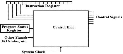
The Control Unit
“Time is nature’s way of keeping everything
from happening at once”
Woody
Allen
We now turn our attention to a
discussion of the control unit, which is that part of the Central Processing
Unit that causes the machine language to take effect. It does this by reacting to the machine
language instruction in the Instruction Register, the status flags in the
Program Status Register, and the interrupts in order to produce control signals that direct the
functioning of the computer.
The main strategy for the
control unit is to break the execution of a machine language instruction into a
number of discrete steps, and then cause these primitive steps to be executed
sequentially in the order appropriate to achieve the affect of the instruction.
The System Clock
The main tool for generating a sequence of basic execution steps is the system
clock, which generates a periodic signal used to generate time steps. In some designs the execution of an
instruction is broken into major phases (e.g., Fetch and Execute), each of
which is broken into a fixed number of minor phases that corresponds to a time
signal. In other systems, the idea of
major and minor phases is not much used.
This figure shows a typical representation of a system clock; the CPU
“speed” is just the number of clock cycles per second.
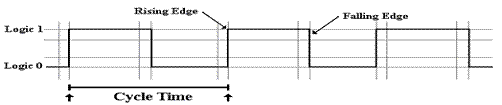
The student should not be
mislead into believing that the above is an actual representation of the
physical clock signal. A true electrical
signal can never rise instantaneously or fall instantaneously. This is a logical representation of the clock
signal, showing that it changes periodically between logic 0 and logic 1. Although the time at logic 1 is commonly the
same as the time at logic 0, this is not a requirement.
Two
Types of Control Units
The function of the control unit is to emit control
signals. We now ask how the control unit
works. A detailed study of the control
unit should be the topic for another course, but we may make a few general
remarks at this time.
The two
major classes of control unit are hardwired and microprogrammed. In a hardwired control unit, the control
signals are the output of combinational logic (AND, OR, NOT gates, etc.) that
has the above as input. The system clock
drives a binary counter that breaks the execution cycle into a number of
states. As an example, there will be a
fetch state, during which control signals are emitted to fetch the instruction
and an execute state during which control signals are emitted to execute the instruction
just fetched.
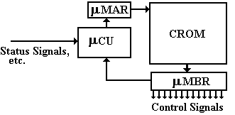
In a microprogrammed control
unit, the control signals are the output of a register called the micro-memory
buffer register. The control program
(or microcode) is just a collection of words in the micro-memory
or CROM (Control Read-Only Memory).
The control unit is sequenced by loading a micro-address into the m–MAR, which causes the
corresponding control word to be placed into the m–MBR
and the control signals to be emitted.
In many ways, the control program
appears to be written in a very primitive machine language, corresponding to a
very primitive assembly language. As an
example, we show a small part of the common fetch microcode from a paper design
called the Boz–5. Note that the memory
is accessed by address and that each micro–word contains a binary number, here
represented as a hexadecimal number.
This just a program that can be changed at will, though not by the
standard CPU write–to–memory instructions.
Address Contents
0x20 0x0010 2108 2121
0x21 0x0011 1500 2222
0x22 0x0006 4200 2323
0x23 0x0100 0000 0000
Microprogrammed
control units are more flexible than hardwired control units because they can
be changed by inserting a new binary control program. As noted in a previous chapter, this
flexibility was quickly recognized by the developers of the System/360 as a
significant marketing advantage. By
extending the System/360 micromemory (not a significant cost) and adding
additional control code, the computer could either be run in native mode as a
System/360, or in emulation mode as either an IBM 1401 or an IBM 7094. This ability to run the IBM 1401 and IBM 7094
executable modules with no modification simplified the process of upgrading
computers and made the System/360 a very popular choice.
It is
generally agreed that the microprogrammed units are slower than hardwired
units, although some writers dispute this.
The disagreement lies not in the relative timings of the two control
units, but on a critical path timing analysis of a complete CPU. It may be that some other part of the
Fetch/Execute cycle is dominating the delays in running the program.
Interrupts and Interrupt Handling
The
standard idea of a stored program computer is that it fetches machine language
instructions sequentially from memory and executes each in order until the
program has terminated. Such a
simplistic strategy will not suffice for modern computation.
Consider
the case of I/O processing. Let us focus
on the arrival of an Ethernet frame at the Network Interface Card (NIC). The data in the frame must be stored in
primary computer memory for later processing before being overwritten. In order to do this, the program under
execution must be suspended temporarily while the program controlling the NIC
starts the data transfer. The primary
mechanism for suspending one program in order to execute another program is
called an interrupt.
The primary
rule for processing interrupts is that the execution of the interrupted program
must not be disrupted; only delayed. There
is a strategy for handling interrupts that works for all I/O interrupts. This is a modification of the basic
instruction fetch cycle. Here it is:
1) At
the beginning of each instruction fetch state, the status of the interrupt line
is tested. In general, this is an active–low signal.
2) If
the interrupt signal has been asserted, the CPU saves the current state of the
CPU,
which is that set of
information required to restart the program as if it had not been
suspended. The CPU then fetches the first instruction of
the interrupt handler routine.
3) The
interrupt handler identifies the source of the interrupt and calls the handler
associated with the device
that raised the interrupt.
4) When
the interrupt handler has finished its job, it terminates and the CPU resumes
the execution of the suspended
program. Since the complete state of the
suspended
program has been saved, it
resumes execution as it nothing had happened.
Virtual Memory and Interrupt
Handling
There is
one situation under which the above–mentioned interrupt strategy is not
adequate. This occurs in a virtual
memory scenario, in which a program can issue addresses that do not correspond
to physical memory. Here are the rules:
1) the
program issues logical addresses,
2) the
address is converted to a physical
address by the operating system,
3) if
the physical address is not in physical memory, a page fault is raised. This
is an
interrupt that can occur after
the instruction fetch phase has completed.
Consider
the execution of a memory–to–memory transfer instruction, such as an assembly
language instruction that might correspond to the high–level language statement
Y
= X. The microprogram to implement
this instruction might appear as follows.
1. Fetch
and decode the instruction.
2. Compute
the address for the label X and fetch the value stored at that address.
Store that value in a
temporary CPU register.
3. Compute
the address for the label Y and store the value from the temporary
CPU register into that
address.
The
IBM S/360 and S/370 architecture contains a number of assembly language
instructions of precisely this format.
The following two instructions are rather commonly used.
MVC (Move
Characters) Moves a string of
characters from one
memory
location to another.
ZAP (Zero
and Add Packed) Moves a sequence of
packed decimal digits
from
one memory location to another.
In each
scenario, the problem is the same. Here
is an analysis of the above sequence.
1. The
instruction is fetched. If the
instruction is located in a page that is not resident
in primary memory, raise a
page fault interrupt. This program is
suspended until
the page with the instruction
is loaded into memory. This is not a
problem.
2. The
argument X
is fetched. If the address of X
is not resident in primary memory,
raise a page fault interrupt. The program is suspended until the page with
the needed
data is loaded into
memory. The instruction is restarted at
step 1. Since the page
containing the instruction is
also memory resident, this is not a problem.
3. The
address of Y is computed.
If that address is not in primary memory, there is
a problem. The instruction has already partially
executed. What to do with the
partial results? In this case, the answer is quite easy,
because the instruction has
had no side effects other than
changing the value of a temporary register: raise a
page fault interrupt, wait for
the page to be loaded, and restart the instruction.
The
handling of such interrupts that can occur after the instruction has had other
side effects, such as storing a partial result into memory, can become quite
complex.
As an
aside, the IBM S/360 did not support virtual memory, which was introduced with
the
S/370 in 1970.
Input/Output Processing
We now consider realistic modes
of transferring data into and out of a computer. We first discuss the limitations of program
controlled I/O and then explain other methods for I/O.
As the
simplest method of I/O, program controlled I/O has a number of shortcomings
that should be expected. These
shortcomings can be loosely grouped into two major issues.
1) The imbalance in the speeds of input and
processor speeds.
Consider keyboard input. An excellent
typist can type about 100 words a minute (the author of these notes was tested
at 30 wpm – wow!), and the world record speeds are 180 wpm (for 1 minute) in
1918 by Margaret Owen and 140 wpm (for 1 hour with an electric typewriter) in
1946 by Stella Pajunas. Consider a
typist who can type 120 words per minute – 2 words a second. In the world of typing, a word is defined to
be 5 characters, thus our excellent typist is producing 10 characters per
second or 1 character every 100,000 microseconds. This is a waste of time; the computer could
execute almost a million instructions if not waiting.
2) The fact that all I/O is initiated by the
CPU.
The other way to state this is that the I/O unit cannot initiate the I/O. This design does not allow for alarms or
error interrupts. Consider a fire alarm. It would be possible for someone at the fire
department to call once a minute and ask if there is a fire in your building;
it is much more efficient for the building to have an alarm system that can be
used to notify the fire department.
Another good example is a patient monitor that alarms if either the
breathing or heart rhythm become irregular.
While such a monitor should be polled by the computer on a frequent
basis, it should be able to raise an alarm at any time.
As a result
of the imbalance in the timings of the purely electronic CPU and the
electro-mechanical I/O devices, a number of I/O strategies have evolved. We shall discuss these in this chapter. All modern methods move away from the designs
that cause the CPU to be the only component to initiate I/O.
The first
idea in getting out of the problems imposed by having the CPU as the sole
initiator of I/O is to have the I/O device able to signal when it is ready for
an I/O transaction. Specifically, we
have two possibilities.
1) The
input device has data ready for reading by the CPU. If this is the case, the CPU
can issue an input
instruction, which will be executed without delay.
2) The
output device can take data from the CPU, either because it can output the data
immediately or because it can
place the data in a buffer for output later.
In this case,
the CPU can issue an output
instruction, which will be executed without delay.
The idea of involving the CPU
in an I/O operation only when the operation can be executed immediately is the
basis of what is called interrupt-driven
I/O. In such cases, the CPU manages
the I/O but does not waste time waiting on busy I/O devices. There is another strategy in which the CPU
turns over management of the I/O process to the I/O device itself. In this strategy, called direct memory access or DMA,
the CPU is interrupted only at the start and termination of the I/O. When the I/O device issues an interrupt
indicating that I/O may proceed, the CPU issues instructions enabling the I/O
device to manage the transfer and interrupt the CPU upon normal termination of
I/O or the occurrence of errors.
An Extended (Silly) Example of I/O Strategies
There are
four major strategies that can be applied to management of the I/O process:
Program-Controlled, and
Interrupt-Driven, and
Direct Memory Access, and
I/O Channel.
We try to
clarify the difference between these strategies by the example of having a
party in one’s house to which guests are invited. The issue here is balancing work done in the
house to prepare it for the party with the tasks of waiting at the front door
to admit the guests.
Program-Controlled
The analogy for
program-controlled I/O would be for the host to remain at the door, constantly
looking out, and admitting guests as each one arrives. The host would be at the door constantly
until the proper number of guests arrived, at which time he or she could
continue preparations for the party.
While standing at the door, the host could do no other productive
work. Most of us would consider that a
waste of time.
Interrupt-Driven
Many of us have
solved this problem by use of an interrupt mechanism called a doorbell. When the doorbell rings, the host suspends
the current task and answers the door.
Having admitted the guest, the host can then return to preparations for
the party. Note that this example
contains, by implication, several issues associated with interrupt handling.
The first issue is priority. If the host
is in the process of putting out a fire in the kitchen, he or she may not
answer the door until the fire is suppressed.
A related issue is necessary completion.
If the host has just taken a cake out of the oven, he or she will not
drop the cake on the floor to answer the door, but will first put the cake down
on a safe place and then proceed to the door.
In this scenario, the host’s time is spent more efficiently as he or she
spends little time actually attending the door and can spend most of the time
in productive work on the party.
Direct Memory Access
In this case, the
host unlocks the door and places a note on it indicating that the guests should
just open the door and come in. The host
places a number of tickets at the door, one for each guest expected, with a
note that the guest taking the last ticket should so inform the host. When the guest taking the last ticket has
arrived, the host is notified and locks the door. In this example the host’s work is minimized
by removing the requirement to go to the door for each arrival of a guest. There are only two trips to the door, one at
the beginning to set up for the arrival of guests and one at the end to close
the door.
I/O Channel
The host hires a
butler to attend the door and lets the butler decide the best way to do
it. The butler is expected to announce
when all the guests have arrived.
Note that the I/O channel is not really a distinct
strategy. Within the context of our
silly example, we note that the butler will use one of the above three
strategies to admit guests. The point of
the strategy in this context is that the host is relieved of the duties. In the real world of computer I/O, the central
processor is relieved of most I/O management duties.
Implementation of I/O
Strategies
We begin our brief discussion of
physical I/O by noting that it is based on interaction of a CPU and a set of
registers associated with the I/O device.
In general, each I/O device has three types of registers associated with
it: data, control, and status. From the
view of a programmer, the I/O device can be almost completely characterized by
these registers, without regard to the actual source or destination of the data.
For
this section, we shall imagine a hopelessly simplistic computer with a single
CPU register, called the ACC (accumulator) and four instructions. These instructions are:
1. LOAD
Address Loads the
accumulator from the memory address,
2. STORE
Address Stores the
accumulator contents into the memory address,
3. GET
Register Loads the
accumulator from the I/O register, and
4. PUT
Register Stores the
accumulator contents into the I/O register.
The best
way to understand IBM’s rationale for its I/O architecture to consider some
simpler designs that might have been chosen.
We begin with a very primitive I/O scheme.
The First Idea, and Why It Cannot Work
At first
consideration, I/O in a computer system would appear trivial. We just issue the instructions and access the
data register by address, so that we have:
GET TEXT_IN_DATA -- this
reads from the input unit.
PUT TEXT_OUT_DATA -- this
writes to the output unit.
Strictly
speaking, these instructions operate as advertised in the code fragments above. We now expose the difficulties, beginning
with the input problem. The input unit
is connected to the CPU through the register at address TEXT_IN_DATA. Loading a CPU from that input register will
always transfer some data, but might not transfer what we want. Normally, we expect an input request to wait
until a character has been input by the user and only then transfer the
character to the CPU. As written above,
the instruction just copies what is in the data buffer of the input unit; it
might be user data or it might be garbage left over from initialization. We must find a way to command the unit to
read, wait for a new character to have been input, and only then transfer the
data to the CPU.
The output
instruction listed above might as well be stated as “Just throw it over the
wall and hope someone catches it.” We
are sending data to the output unit without first testing to see if the output
unit is ready for data. Early in his
career as a programmer, this author wrote a program that sent characters to a
teletype printer faster than they could be printed; the result was that each
character printed was a combination of two or more characters actually sent to
the TTY, and none were actually correct.
As this was the intended result of this experiment, this author was
pleased and determined that he had learned something.
The
solution to the problem of actually being able to do input and output correctly
is based on the proper use of these two instructions. The solution we shall describe is called program controlled I/O. We shall first describe the method and then
note its shortcomings.
The basic
idea for program–controlled I/O is
that the CPU initiates all input and output operations. The CPU must test the status of each device
before attempting to use it and issue an I/O command only when the device is
ready to accept the command. The CPU
then commands the device and continually checks the device status until it
detects that the device is ready for an I/O event. For input, this happens when the device has
new data in its data buffer. For output,
this happens when the device is ready to accept new data.
Pure
program–controlled I/O is feasible only when working with devices that are
always instantly ready to transfer data.
For example, we might use program–controlled input to read an electronic
gauge. Every time we read the gauge, the
CPU will get a value. While this
solution is not without problems, it does avoid the busy wait problem.
The “busy wait” problem occurs when the CPU
executes a tight loop doing nothing except waiting for the I/O device to
complete its transaction. Consider the
example of a fast typist inputting data at the rate of one character per
100,000 microseconds. The busy wait loop
will execute about one million times per character input, just wasting
time. The shortcomings of such a method
are obvious (IBM had observed them in the late 1940’s).
As a result
of the imbalance in the timings of the purely electronic CPU and the electro–mechanical
I/O devices, a number of I/O strategies have evolved. We shall discuss these in this chapter. All modern methods move away from the designs
that cause the CPU to be the only component to initiate I/O.
The idea of
involving the CPU in an I/O operation only when the operation can be executed
immediately is the basis of what is called interrupt-driven
I/O. In such cases, the CPU manages
the I/O but does not waste time waiting on busy I/O devices. There is another strategy in which the CPU
turns over management of the I/O process to the I/O device itself. In this strategy, called direct memory access or DMA,
the CPU is interrupted only at the start and termination of the I/O. When the I/O device issues an interrupt
indicating that I/O may proceed, the CPU issues instructions enabling the I/O
device to manage the transfer and interrupt the CPU upon normal termination of
I/O or the occurrence of errors.
Interrupt Driven I/O
Here the
CPU suspends the program that requests the Input and activates another
process. While this other process is being
executed, the input device raises 80 interrupts, one for each of the characters
input. When the interrupt is raised, the
device handler is activated for the very short time that it takes to copy the
character into a buffer, and then the other process is activated again. When the input is complete, the original user
process is resumed.
In a
time–shared system, such as all of the S/370 and successors, the idea of an
interrupt allows the CPU to continue with productive work while a program is
waiting for data. Here is a rough scenario
for the sequence of events following an I/O request by a user job.
1. The
operating system commands the operation on the selected I/O device.
2. The
operating system suspends execution of the job, places it on a wait queue,
and assigns the CPU to another
job that is ready to run.
3. Upon
completion of the I/O, the device raises an interrupt. The operating system
handles the interrupt and
places the original job in a queue, marked as ready to run.
4. At
some time later, the job will be run.
In order to
consider the next refinement of the I/O structure, let us consider what we have
discussed previously. Suppose that a
line of 80 typed characters is to be input.
Interrupt Driven
Here the
CPU suspends the program that requests the Input and activates another
process. While this other process is
being executed, the input device raises 80 interrupts, one for each of the
characters input. When the interrupt is
raised, the device handler is activated for the very short time that it takes
to copy the character into a buffer, and then the other process is activated
again. When the input is complete, the
original user process is resumed.
Direct Memory Access
DMA is a refinement of interrupt-driven
I/O in that it uses interrupts at the beginning and end of the I/O, but not
during the transfer of data. The
implication here is that the actual transfer of data is not handled by the CPU
(which would do that by processing interrupts), but by the I/O controller
itself. This removes a considerable
burden from the CPU.
In the DMA
scenario, the CPU suspends the program that requests the input and again
activates another process that is eligible to execute. When the I/O device raises an interrupt
indicating that it is ready to start I/O, the other process is suspended and an
I/O process begins. The purpose of this
I/O process is to initiate the device I/O, after which the other process is
resumed. There is no interrupt again
until the I/O is finished.
The design
of a DMA controller then involves the development of mechanisms by which the
controller can communicate directly with the computer’s primary memory. The controller must be able to assert a
memory address, specify a memory READ or memory WRITE, and access the primary
data register, called the MBR (Memory Buffer Register).
Immediately,
we see the need for a bus arbitration
strategy – suppose that both the CPU and a DMA controller want to access
the memory at the same time. The
solution to this problem is called “cycle
stealing”, in which the CPU is blocked for a cycle from accessing the
memory in order to give preference to the DMA device.
Any DMA
controller must contain at least four registers used to interface to the system
bus.
1) A
word count register (WCR) – indicating how many words to transfer.
2) An
address register (AR) – indicating the memory address to be used.
3) A
data buffer.
4) A
status register, to allow the device status to be tested by the CPU.
In essence,
the CPU tells the DMA controller “Since you have interrupted me, I assume that
you are ready to transfer data. Transfer
this amount of data to or from the memory block beginning at this memory
address and let me know when you are done or have a problem.”
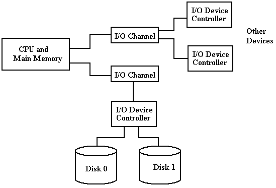
I/O Channel
A channel
is a separate special-purpose computer that serves as a sophisticated Direct
Memory Access device controller. It
directs data between a number of I/O devices and the main memory of the
computer. Generally, the difference is
that a DMA controller will handle only one device, while an I/O channel will
handle a number of devices.
The I/O
channel concept was developed by IBM (the International Business Machine
Corporation) in the 1940’s because it was obvious even then that data
Input/Output might be a real limit on computer performance if the I/O
controller were poorly designed. By the
IBM naming convention, I/O channels execute channel commands, as opposed to instructions.
There are
two types of channels – multiplexer and selector.
A multiplexer channel supports more
than one I/O device by interleaving the transfer of blocks of data. A byte
multiplexer channel will be used to handle a number of low-speed devices,
such as printers and terminals. A block multiplexer channel is used to
support higher-speed devices, such as tape drives and disks.
A selector channel is designed to handle
high speed devices, one at a time. This
type of channel became largely disused prior to 1980, probably replaced by
blocked multiplexers.
Each I/O
channel is attached to one or more I/O devices through device controllers that
are similar to those used for Interrupt-Driven I/O and DMA, as discussed above.
I/O Channels, Control Units, and I/O
Devices
In one
sense, an I/O channel is not really a distinct I/O strategy, due to the fact
that an I/O channel is a special purpose processor that uses either
Interrupt-Driven I/O or DMA to affect its I/O done on behalf of the central
processor. This view is unnecessarily
academic.
In the IBM
System-370 architecture, the CPU initiates I/O by executing a specific instruction
in the CPU instruction set: EXCP for Execute
Channel Program. Channel programs
are essentially one word programs that can be “chained” to form multi-command sequences.
Physical IOCS
The low
level programming of I/O channels, called PIOCS
for Physical I/O Control System, provides for channel scheduling, error
recovery, and interrupt handling. At
this level, the one writes a channel program (one or more channel command
words) and synchronizes the main program with the completion of I/O operations.
For example, consider double-buffered I/O, in which a data
buffer is filled and then processed while another data buffer is being
filled. It is very important to verify
that the buffer has been filled prior to processing the data in it.
In the IBM
PIOCS there are four major macros used to write the code.
CCW Channel Command Word
The CCW
macro causes the IBM assembler to construct an 8-byte channel command
word. The CCW includes the I/O command
code (1 for read, 2 for write, and other values), the start address in main
memory for the I/O transfer, a number of flag bits, and a count field.
EXCP Execute Channel Program
This macro
causes the physical I/O system to start an I/O operation. This macro takes as its single argument the
address of a block of channel commands to be executed.
WAIT
This
synchronizes main program execution with the completion of an I/O
operation. This macro takes as its
single argument the address of the block of channel commands for which it will
wait.
Chaining
The PIOCS
provides a number of interesting chaining options, including command
chaining. By default, a channel program
comprises only one channel command word.
To execute more than one channel command word before terminating the I/O
operation, it is necessary to chain each command word to the next one in the
sequence; only the last command word in the block does not contain a chain bit.
Here is a sample of I/O code.
The main
I/O code is as follows. Note that the
program waits for I/O completion.
// First execute the channel program at
address INDEVICE.
EXCP INDEVICE
// Then wait to synchronize program
execution with the I/O
WAIT INDEVICE
// Fill three arrays in sequence, each with
100 bytes.
INDEVICE CCW 2,
ARRAY_A, X’40’, 100
CCW 2, ARRAY_B, X’40’, 100
CCW 2, ARRAY_C, X’00’, 100
The first number in the CCW (channel command word) is the command
code indicating the operation to be performed; e.g., 1 for write and 2 for
read. The hexadecimal 40 in the CCW is
the “chain command flag” indicating that the commands should be chained. Note that the last command in the list has a
chain command flag set to 0, indicating that it is the last one.
Front End Processor
We can push
the I/O design strategy one step further – let another computer handle it. One example that used to be common occurred
when the IBM 7090 was introduced. At the
time, the IBM 1400 series computer was quite popular. The IBM 7090 was designed to facilitate
scientific computations and was very good at that, but it was not very good at
I/O processing. As the IBM 1400 series
excelled at I/O processing it was often used as an I/O front-end processor,
allowing the IBM 7090 to handle I/O only via tape drives.
The batch
scenario worked as follows:
1) Jobs
to be executed were “batched” via the IBM 1401 onto magnetic tape. This
scenario did not support time
sharing.
2) The
IBM 7090 read the tapes, processed the jobs, and wrote results to tape.
3) The
IBM 1401 read the tape and output the results as indicated. This output
included program listings and
any data output required.
Another
system that was in use was a combined CDC 6400/CDC 7600 system (with computers
made by Control Data Corporation), in which the CDC 6400 operated as an I/O
front-end and wrote to disk files for processing by the CDC 7600. This combination was in addition to the fact
that each of the CDC 6400 and CDC 7600 had a number of IOPS (I/O Processors)
that were essentially I/O channels as defined by IBM.
Gulliver’s Travels and “Big-Endian” vs. “Little-Endian”
The author
of these notes has been told repeatedly of the literary antecedents of the
terms “big-endian” and “little-endian” as applied to byte ordering in
computers. In a fit of scholarship, he
decided to find the original quote. Here
it is, taken from Chapter IV of Part I (A Voyage to Lilliput) of Gulliver’s
Travels by Jonathan Swift, published October 28, 1726.
The edition
consulted for these notes was published in 1958 by Random House, Inc. as a part
of its “Modern Library Books” collection.
The LC Catalog Number is 58-6364.
The story
of “big-endian” vs. “little-endian” is described in the form on a conversation
between Gulliver and a Lilliputian named Reldresal, the Principal
Secretary of Private Affairs to the Emperor of Lilliput. Reldresal is presenting a history of a
number of struggles in Lilliput, when he moves from one difficulty to
another. The following quote preserves
the unusual capitalization and punctuation found in the source material.
“Now, in the midst of these intestine Disquiets, we are
threatened with an Invasion from the Island of Blefuscu, which is the
other great Empire of the Universe, almost as large and powerful as this of his
majesty. ….
[The two great Empires of Lilliput and Blefuscu]
have, as I was going to tell you, been engaged in a most obstinate War for six
and thirty Moons past. It began upon the
following Occasion. It is allowed on all
Hands, that the primitive Way of breaking Eggs before we eat them, was upon the
larger End: But his present Majesty’s Grand-father, while he was a Boy, going
to eat an Egg, and breaking it according to the ancient Practice, happened to
cut one of his Fingers. Whereupon the
Emperor his Father, published an Edict, commanding all his Subjects, upon great
Penalties, to break the smaller End of their Eggs. The People so highly resented this Law, that
our Histories tell us, there have been six Rebellions raised on that Account;
wherein one Emperor lost his Life, and another his Crown. These civil Commotions were constantly
fomented by the Monarchs of Blefuscu; and when they were quelled, the
Exiles always fled for Refuge to that Empire.
It is computed, that eleven Thousand Persons have, at several Times,
suffered Death, rather than submit to break their Eggs at the smaller end. Many hundred large Volumes have been
published upon this Controversy: But the Books of the Big-Endians have
been long forbidden, and the whole Party rendered incapable by Law of holding
Employments.”
Jonathan
Swift was born in Ireland
in 1667 of English parents. He took a
B.A. at Trinity College in Dublin and some time later was ordained an Anglican
priest, serving briefly in a parish church, and became Dean of St. Patrick’s in
Dublin in 1713. Contemporary critics
consider the Big-Endians and Little-Endians to represent Roman Catholics and
Protestants respectively. Lilliput seems
to represent England, and
its enemy Blefuscu is variously considered to represent either France or Ireland. Note that the phrase “little-endian” seems
not to appear explicitly in the text of Gulliver’s Travels.
