Declaring Binary Storage
There are many ways to declare binary storage. The four most useful are
1. B Ordinary binary,
2. F Full–word (32–bit binary two’s–complement integer),
3. H Half–word (16–bit) binary two’s–complement integer), and
4. X Hexadecimal.
Each
of the B and X declarations may declare a storage area with length from 1
through 256 bytes. The lengths of the F
and H declarations are fixed at 4 and 2 bytes respectively.
Apparently, it is possible to assign a length in bytes to either type, but this
is strange.
Note that the two declarations below have an identical effect. Each defines a 32–bit binary integer with value equal to 14,336 in decimal.
F1 DC F‘14336’ DEFAULT SIZE IS FOUR BYTES.
X1 DC XL4‘00003800’ SIZE SPECIFIED AS FOUR BYTES.
While the second declaration is unusual for a full–word, it makes some examples easier.
More On DC (Define Constant)
The general format of the DC statement is as follows.
|
Name |
DC |
dTLn ‘constant’ |
The name is an optional entry, but required if the program is to refer to the field by name. The standard column positions apply here.
The declarative, DC, comes next in its standard position.
The entry “dTLn” is read as follows.
d is the optional duplication factor. If not specified, it defaults to 1.
T is
the required type specification. The
types for binary are B, F, H, and X.
Note that the data actually
stored at the location does not need to be
of this type, but it is a
good idea to restrict it to that type.
L is an optional length of the data field in bytes.
The
‘constant’ entry is required and is used to specify a value. If the length attribute is omitted, the
length is specified implicitly by this entry.
Again, it is rarely desirable
to specify a length for the F and H data types.
Alignment and
Remember
that the System/360 is a byte–addressable machine. The type F declares a full–word, which is a
four–byte field aligned on a full–word boundary; i.e., its address is a
multiple of four. The type H declares a
half–word, which is a two–byte field aligned on a
half–word boundary; i.e., its address is a multiple of two.
If the value declared
in either a type F or type H constant is greater than that
allowed by the data type, the assembler merely truncates the leftmost digits.
Consider the following example
BAD DC H‘73728’ IN HEXADECIMAL, X‘12000’
This
is truncated to a value of 8,192, which is X‘2000’. The leading 1 is dropped
from the hexadecimal representation, because only the last four digits fit into
the
half–word storage allocation; 4 hexadecimal digits = 2 bytes = 1 half–word.
Sequential Memory
Consider
the following two declarations which are sequential. Each is a half–word,
which is declared using the hexadecimal construct to make the example clear.
H1 DC XL2‘0102’
DECIMAL 258
H2 DC
XL2‘0304’ DECIMAL 772 At address H1+2
The half–word value stored at address H1 is hexadecimal 0102 or decimal 258.
The
full–word value stored at address H1 is hexadecimal 01020304, or
16,
909, 060 in decimal. This fact
can present problems for the incautious coder.
To
load the value of the half–word at address H1 into a register, one uses the Load
Half–word instruction; e.g., LH R4,H1. Register R4 gets 258. But if I accidentally write a full–word load
instruction, as in L R4,H1, then register R4 will get
the decimal value
16, 909, 060. This is due to the fact
that the four bytes beginning at address H1 have the value X‘0102 0304’. The fact that H1 and H2 are defined
separately matters not at all.
Similarly, suppose I declare a full–word as follows.
F1 DC
XL4 ‘11121314’ DECIMAL 17,899,828
If the code says LH R4,F1, then F1 gets hexadecimal X‘1112’ or decimal 4370.
Binary Constants and Hexadecimal Constants
The type B declaration uses binary numbers (0 or 1) to define a string of bits. The type X declaration uses hexadecimal digits to define what is also just a string of bits.
Consider the following pairs of declarations.
B1 DC B‘10101110’
X1 DC XL1‘AE’ READ AS 1010 1110
B2 DC B‘0001001000010011’
X2 DC XL2‘1213’ READ AS 0001 0010 0001 0011
B1 and X1 each declare the same bit pattern.
B2 and X2 each declare the same bit pattern.
Personally, I find the hexadecimal constants much easier to read, and would suggest not using the B declaration. The most common use for the binary declaration would be to set bit patterns to be sent to registers that control Input/Output devices. In standard programming, we do not have access to those registers on a System/360 or later mainframe..
Input and Output of Binary Data
All data are input originally as EBCDIC characters.
All data printed must be output as EBCDIC characters.
The
standard input process for binary data is a two–step one, in which the
character
data are first packed to form decimal data and then converted to binary.
The
standard process to output binary data from a register is also a two–step one.
First convert the binary to decimal data and then use unpack or the edit
instruction
to produce the printable EBCDIC characters.
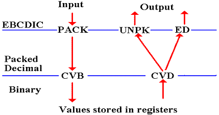
Conversion between Packed Decimal and Binary
These two conversion instructions are each a type RX instruction.
CVB (Convert to Binary) converts packed decimal data from storage into binary form in a general–purpose register. This is a type RX instruction with opcode X‘4F’.
CVD (Convert to Decimal) converts binary data in a general–purpose register into packed decimal form in storage. This is a type RX instruction with opcode X‘4E’.
The format of each is OP R1,D2(X2,B2).
Template for the instructions: CVB Register,Storage_Location
CVD
Register,Storage_Location
For
the CVB instruction, the Storage Location contains the packed decimal value
that
is to be converted to binary and placed in the register.
For the CVD instruction, the Storage Location is the field that will receive the packed decimal value resulting from the conversion of the value in the register.
It
is standard practice to use the floating point data type D (double word) to
declare the storage location.
Why A Floating Point Type Here?
The D data type declares a double precision floating point value, which occupies eight bytes (64 bits) and is automatically aligned on a double–word boundary. In other words, its address is a multiple of 8. The true requirement for the operand is that it be exactly eight bytes long and begin on a double–word boundary. The D declaration fills the bill.
Consider the following code, which is rather standard.
CVB
R6,D1
D1
DS D DOUBLE WORD OR 8 BYTES
One might also write the following, if one is careful.
CVB
R6,D2
D2
DS PL8 EIGHT BYTES FOR UP TO 15
DIGITS
The
difficulty here is insuring that D2 is properly aligned on a double–word
boundary.
While this can be done, it is less error–prone to use the D type and have the
assembler
automatically do the alignment for you.
Example and Comments
How
many digits do I really need? The
biggest value storable as a 32–bit binary number is 2,147,483,647. This number has 10 digits, which will be
converted to 11 digits for storage in
Packed Decimal format. A 4–byte
full–word will store only seven digits.
It takes a six–byte packed decimal field to store 11 digits. There is no data size that automatically
takes 6 bytes and no provision for aligning an address on a multiple of
six. The obvious choice for the packed
decimal intermediary form is storage as a double–word.
Input example
ZAP
D1,AMTPACK TRANSFER TO THE DOUBLE
WORD
CVB
R5,D1 CONVERT TO BINARY
D1 DS
D THIS RESERVES EIGHT
BYTES
Output example
CVD R5,
ZAP AMTPACK,D2 TRANSFER TO THE PACKED WORD
D2 DS
D THIS ALSO RESERVES
EIGHT BYTES
Each of these examples assumes that a field, AMTPACK in each, has been properly declared with the proper length. Recall that each example is a part of a larger process.
The
input process has several steps:
1. Read
in the sequence of digits as EBCDIC characters.
2. Use
the PACK command to place the result in the field AMTPACK.
3. Use
the above sequence to convert the number to binary form in the register.
The
output process has several steps:
1. Use
the above sequence to convert the binary number in the register to
a packed form in the field AMTPACK.
2. Use
UNPK or ED, preferably the latter, to generate the EBCDIC characters
that form the printable
output.
RX (Register–Indexed Storage): Explicit Base Register Usage
This is a four–byte instruction of the form OP R1,D2(X2,B2).
|
Type |
Bytes |
Operands |
1 |
2 |
3 |
4 |
|
RX |
4 |
R1,D2(X2,B2) |
OP |
R1 X2 |
B2 D2 |
D2D2 |
The first byte contains the 8–bit instruction code.
The second byte contains two 4–bit fields, each of which encodes a register number. The first hexadecimal digit, denoted R1, identifies the register to be used as either the source or destination for the data. The second hexadecimal digit, denoted X2, identifies the register to be used as the index. If the value is 0, indexed addressing is not used.
The third and fourth bytes contain a standard address in base/displacement format.
As an
examples of this type, we consider the two following instructions:
L Load Fullword Opcode is X‘58’
A Add Fullword Opcode is X‘5A’
We consider a number of examples based on the following data declarations. Note that the data are defined in consecutive fullwords in memory, so that fixed offset addressing can be employed. Each fullword has a length of four bytes.
DAT1 DC
F‘1111’
DAT2 DC F‘2222’ AT ADDRESS (DAT1 + 4)
DAT3 DC F‘3333’ AT ADDRESS (DAT2 + 4) OR (DAT1 + 8)
A standard code block might appear as follows.
L R5,DAT1
A R5,DAT2
A R5,DAT3 NOW HAVE THE SUM.
One variant of this code might be the following. See page 92 of R_17.
LA R3,DAT1 GET ADDRESS INTO R3
L
R5,0(,3) LOAD DAT1 INTO R5
A R5,4(,3)
ADD DAT2, AT ADDRESS DAT1+4.
A
R5,8(,3) ADD DAT3, AT ADDRESS
DAT1+8.
Note the leading comma in the construct (,3), which is of the form (Index, Base). This indicates that no index register is being used, but that R3 is being used as a base register. It is equivalent to the construct (0,3), which might be preferred.
Here is another variant of the above code.
LA R3,DAT1 GET ADDRESS INTO R3
LA R8,4 VALUE 4 INTO REGISTER 8
LA R9,8 VALUE 8 INTO REGISTER 9
L
R5,0(0,3) LOAD DAT1 INTO R5
A R5,0(8,3)
ADD DAT2, AT ADDRESS DAT1+4.
A
R5,0(9,3) ADD DAT3, AT ADDRESS
DAT1+8.
Loading Values: L, LH, LR, and LCR
The general–purpose registers are designed to store and manipulate binary data that are stored in the form of 32–bit two’s–complement integers. As an aside, remember two facts about such numbers.
1. The IBM standard
is to number the bits from left to right as 0 through 31.
The sign bit is called “Bit
0” and the units bit on the right “Bit 31”.
2. IBM
will often call this “31 bit data”, as the value has a 31–bit magnitude
(stored in bits 1 – 31) and
a sign bit.
We first discuss three of the standard instructions used to load values into a register.
L Load a full–word value into the register.
LH Load
a half–word value into the register.
The 16–bit value
is sign extended into 32–bits for the register.
LR Copy a value from one register to another register.
LCR Load the first register with the two’s–complement of the value in the second.
Note: None of these instructions will set a condition code.
Do not load a register and expect a condition code to reflect the value loaded.
L (Load 32–bit Full–word)
The instruction is a type RX, with format L R1,D2(X2,B2). The opcode is X‘58’. The object code format is as follows.
|
Type |
Bytes |
Operands |
1 |
2 |
3 |
4 |
|
RX |
4 |
R1,D2(X2,B2) |
X‘58’ |
R1 X2 |
B2 D2 |
D2D2 |
The first operand specifies any
general–purpose register. This is
indicated by the first
hexadecimal digit in the second byte of the object code.
The
second operand references a full–word in storage, usually aligned on a
full–word
boundary. If the second operand is a
literal, the assembler will align it properly.
The address of this second word is computed from the standard
base/displacement form (B2 D2 D2 D2
in bytes 3 and 4) with an index register (the second hexadecimal digit in byte
2).
Here is a template for the instruction: L Reg,Full_Word
Here are some examples of common usage. Other examples will be discussed later.
L1 L R2,=F‘4000’ R2 GETS DECIMAL 4000
L2 L R3,F1 R3 ALSO GETS DECIMAL 4000
L3 L R4,H1 THIS IS PROBABLY A MISTAKE.
L4 L R5,=A(H1) LOAD THE ADDRESS INTO R5.
F1 DC F‘4000’
H1 DC H‘2000’ Stored as X‘07 D0’
H2 DC H‘3000’ Stored as X‘0B B8’
Note again, it is usually a mistake to attempt to use a full–word load to place a half–word value into a register. What will happen when the instruction at address L3 is executed is that register R4 will be loaded with the value X‘07 D0 0B B8’, or decimal 131, 075, 000.
The execution of the instruction at address L4 causes the address of the halfword H1, not its value, to be loaded into register R5. For the System/370, the address is a 24–bit unsigned integer that is extended to a 32–bit value for storage in the register.
LH (Load 16–bit Half–word)
The
instruction is a type RX, with format LH R1,D2(X2,B2). The
opcode is X‘48’.
The object code format is as follows.
|
Type |
Bytes |
Operands |
1 |
2 |
3 |
4 |
|
RX |
4 |
R1,D2(X2,B2) |
X‘48’ |
R1 X2 |
B2 D2 |
D2D2 |
The first operand specifies any
general–purpose register. This is
indicated by the first
hexadecimal digit in the second byte of the object code.
The
second operand references a full–word in storage, usually aligned on a half–word
boundary. If the second operand is a
literal, the assembler will align it properly.
The address of this second word is computed from the standard
base/displacement form (B2 D2 D2 D2
in bytes 3 and 4) with an index register (the second hexadecimal digit in byte
2).
The
assembler loads the half–word into the rightmost 16 bits of the register (16 –
31)
and then propagates the half–word’s sign bit through the left 16 bits of the
register.
Here is a template for the instruction: LH Reg,Half_Word
Here are some examples of common usage. Other examples will be discussed later.
L1 LH R2,=H‘4000’ R2 GETS DECIMAL 4000
L2 LH R3,H1 R3 GETS DECIMAL 2000
L3 LH
R4,F1 THIS IS PROBABLY A MISTAKE.
F1 DC F‘4000’ Stored as X‘00 00 0F A0’
H1 DC H‘2000’
The difficulty with the instruction at address L3 is that it will access the two bytes at the addresses F1 and F1+1. The halfword stored there has value X‘00 00’, or just 0.
Sign Extension for LH
Consider two 16–bit integers that are stored as half–words in two’s–complement form.
The positive number + 100 is stored as 0000 0000 0110 0100, or X‘0064’.
The negative number –100 is stored as 1111 1111 1001 1100 or X‘FF9C’
The LH sign extends the halfword data into fullword data with the proper sign. This it does by copying bits 0 through 15 of the halfword into bits 16 through 31 of the register and then copying the sign bit (now in register bit 16) into bits 0 through 15 of the register.
Consider the code fragment below.
LH R7,=H‘100’
After this, register R7 contains the full–word value +100, as shown below.
|
Left half–word |
Right half–word |
||||||
|
0 – 3 |
4 – 7 |
8 – 11 |
12 – 15 |
16 – 19 |
20 – 23 |
24 – 27 |
28 – 31 |
|
0000 |
0000 |
0000 |
0000 |
0000 |
0000 |
0110 |
0100 |
Now consider the code fragment.
LH R8,=H‘-100’
After this, register R8 contains the full–word value –100, as shown below.
|
Left half–word |
Right half–word |
||||||
|
0 – 3 |
4 – 7 |
8 – 11 |
12 – 15 |
16 – 19 |
20 – 23 |
24 – 27 |
28 – 31 |
|
1111 |
1111 |
1111 |
1111 |
1111 |
1111 |
1001 |
1100 |
LR (Load Register) and LCR (Load Complement Register)
Each instruction is a type RR, with format LR R1,R2. The opcode for LR is X‘18’.
The opcode for LCR is X‘13’. The object code format for each is as follows.
|
Type |
Bytes |
Operands |
|
|
|
RR |
2 |
R1,R2 |
OP |
R1 R2 |
Each operand specifies any general–purpose register. The contents of the register specified as the second operand are copied into the register specified as the first operand.
Consider the code fragment below.
L
R9,=H‘200’ REGISTER 9 GETS
DECIMAL 200
LR R7,R9 REGISTER 7 ALSO GETS 200
THIS TIME IT IS
COPIED FROM R9
LCR R8,R9 REGISTER 8 GETS DECIMAL -200, STORED
IN PROPER 2’S-COMPLEMENT
FORMAT.
LM (Load Multiple Registers)
The LM instruction loads data from main storage into more than one register.
The instruction is a type RS with format LM R1,R3,D2(B2). The opcode is X‘98’.
This is a four–byte instruction with object code format as follows:
|
Type |
Bytes |
Operands |
1 |
2 |
3 |
4 |
|
RS |
4 |
R1,R3,D2(B2) |
X‘98’ |
R1 R3 |
B2 D2 |
D2D2 |
The first byte contains the 8–bit instruction code.
The second byte contains two 4–bit fields, each of which encodes a register number. These two bytes specify the range of registers to be loaded.
The third and fourth bytes together contain a 4–bit register number and 12–bit displacement used to specify the memory address of the operand in storage. This operand is considered as the first fullword a block of fullwords; the size of the block is determined by the number of registers specified in byte 2. This is a type RS instruction; indexed addressing is not used.
Recall
that each label in the assembly language program references an address,
which must be expressed in the form of a base register with displacement.
Any address in the format of base register and displacement will appear in the form.
|
B D1 |
D2 D3 |
B is the hexadecimal digit representing the base register.
The register numbers “wrap around”, so that 15,1 specifies the three registers 15, 0, 1.
Example code:
LM R6,R8,F1 LOAD R6, R7, R8 FROM F1, F2, F3
LM R15,R2,F1 LOAD R15, R0, R1, R2 FROM F1 TO F4
F1 DC F‘1111’
F2 DC F‘2222’
F3 DC F‘3333’
F4 DC F‘4444’
LM and the Standard Closing Code
Look again at part of the standard closing code for our programs.
******************* END LOGIC
**************************
L
R13,SAVEAREA+4 POINT AT
OLD SAVE AREA
LM
R14,R12,12(R13) RESTORE THE REGISTERS
LA
R15,0 RETURN
CODE = 0
BR R14 RETURN TO OPERATING SYSTEM
The
label SAVEAREA
references a sequence of full words used to save information
used when returning to the operating system.
The
second full–word in this area, at address SAVEAREA+4, holds the address of
the block of memory used to save the register information.
The instruction LM R14,R12,12(R13) loads the 15 registers R14 through R12, omitting only R13, with the 15 full–word values beginning at the specified address. More specifically, the old register values are saved in a block beginning with the fourth full–word (at offset 12) in the block with address now in R13. The address 12(R13) is specified in base/displacement format and references the start address of the 60–byte part of the save area that is used to store the values of the registers.
The
instruction LA R15,0 is a use of a Load Address instruction that
we shall discuss
very shortly. I would prefer something
like LH
R15,=H‘0’, which appears to be equivalent, but can lead to
addressability issues. The LA
format is safer.
Loading Addresses
Up to now, we have discussed “value loaders”, such as the following example.
L R3,FW1
This finds the full–word at address FW1 and loads its value into register R3.
At
times, we shall need not the value stored at an address but the address itself.
One possibility would be to store a return address to be used by a subroutine.
There are two common ways to access the address and store it into a register.
1. Use the L (Load full–word) instruction and use an address literal
2. Use the LA (Load Address) instruction and use the label.
The following two statements are equivalent. Each loads R1 with the address FW1.
L R1,=A(FW1)
LA R1,FW1
In the System/360 and
System/370 the address is treated as a 24–bit unsigned integer,
which can be represented by six hexadecimal digits.
If the address of FW1 is X‘112233’, register R1 gets X‘00112233’.
LA (Load Address)
The instruction is a type RX, with format LA R1,D2(X2,B2). The opcode is X‘41’.
The object code format is as follows.
|
Type |
Bytes |
Operands |
1 |
2 |
3 |
4 |
|
RX |
4 |
R1,D2(X2,B2) |
X‘41’ |
R1 X2 |
B2 D2 |
D2D2 |
Here is a template for the instruction: LA Reg,Address
The
first operand specifies any general–purpose register. This is indicated in the
object code by the first hexadecimal digit in the second byte.
The second operand references a storage address in the form D2(X2,B2). The index register is specified by the second hexadecimal digit in the second byte. Bytes 3 and 4 together contain an address in base/displacement form, to which the index value is added.
Consider the following fragment of code, which indicates one use of the instruction.
LA R9,A10
A10 DC F‘100’
Suppose that label A10
is subject to base register 3 containing value X‘9800’
with a displacement of X‘260’. The object code for the LA instruction is as
follows.
41
90 32 60
The
code for the LA instruction is X‘41’. The second byte “90” is of the form
R1X2,
where R1 is the target register and X2 is the index register. As is standard, a value of 0 indicates that
indexing is not used in this address; it is pure base/displacement form.
The LA instruction causes register R9 to be get value X‘9800’ + X‘260’ = X‘9A60’.
LA: A Second Look
The instruction is a type RX, with format LA R1,D2(X2,B2).
Consider the example above, coded as LA R9,X‘260’(0,3).
Again, the object code for this is 41 90 32 60.
Let’s analyze this object code. What it says is the following:
1) Take
the contents of register 3 X‘9800’
2) Add the value of the offset X‘260’
3) Add
the contents of the index X‘000’
(here no index register is
used)
4) Get the value X‘9A60’
5) Place that value into register R9, which now contains X‘0000 9A60’.
But note: While we call this an address, it is really just an unsigned binary number.
This gives rise to
a common use of the LA instruction to load a constant
value into a
general–purpose register.
LA: Load Register with Explicit Value
Consider the instruction LA R8,4(0,0).
The object code for this is 41 80 00 04.
The
code is executed assuming no base register and no index register.
The number 4 is computed and loaded into register 8.
The following instruction is considered identical: LA R8,4.
Note
that the second operand in this form of the instruction is a non–negative
integer that is treated by the assembler as a displacement.
This implies that the value must be in a form that can be represented as a 12–bit unsigned integer, specifically that it must be a non–negative integer not larger than 4,095 (decimal).
Consider now the line from the standard ending code of our programs.
LA
R15,0 RETURN
CODE = 0
This places the value 0 into the destination register.
Instructions: Surface Meaning and Uses
In the previous example, we see a trick that is commonly used by assembly language programmers: find what the instruction really does and exploit it. The surface meaning of the LA instruction is simple: load the address of a label or symbolic address into a given register.
The usage to load a register with a small non–negative constant value is an immediate and logical result of the way the object code is executed. The goals of such tricks seem to be:
1) To gain coding efficiency, and
2) To avoid addressing problems that sometimes arise in the use of literals.
Storing Register Values: ST, STH, and STM
ST (Store Full Word) is a type RX instruction, with format ST R1,D2(X2,B2).
STH (Store Half Word) is a type RX instruction, with format STH R1,D2(X2,B2).
STM (Store Multiple) is a type RS instruction, with format STM R1,R3,D2(B2).
The
ST instruction stores the full–word contents of the register, specified in the
first operand, into the full word at the address specified by the second
operand.
The
STH instruction stores the rightmost 16 bits of the register specified by the
first operand into the half word at the address specified by the second
operand.
For
STM (Store Multiple Registers), the first two operands specify a range of
registers to be stored. Remember that
the register numbers “wrap around”
STM
R7,R10,X2 STORE THE FOUR REGISTERS
R7,R8,R9,AND R10
INTO FOUR FULL-WORDS
BEGINNING AT X2
STM
R10,R7,X4 STORE THE 14 REGISTERS R10 THROUGH
R7
(ALL BUT R8 AND R9) INTO
14 FULL-WORDS
While
each of these instructions is quite similar to its load register partner, we
shall
spend a bit of time discussing the instructions. After all, this is a textbook.
ST: Store Fullword
The
ST (Store Full Word) is a type RX instruction, with format ST R1,D2(X2,B2)
and opcode X‘50’. The
object code format is as follows:
|
Type |
Bytes |
Operands |
1 |
2 |
3 |
4 |
|
RX |
4 |
R1,D2(X2,B2) |
X‘50’ |
R1 X2 |
B2 D2 |
D2D2 |
The first operand specifies any
general–purpose register. This is
indicated by the first
hexadecimal digit in the second byte of the object code.
The
second operand references a full–word in storage, usually aligned on a
full–word
boundary. The address of this second
word is computed from the standard base/displacement form (B2 D2
D2 D2 in bytes 3 and 4) with an index register (the
second hexadecimal digit in byte 2). Here
is a template for the instruction: ST
Reg,Full_Word
Here
are some examples of common usage. Other
examples will be discussed later.
Suppose that R3 contains the decimal value 163840, which is X‘0002
8000’.
F1 DC X‘0000 0000’
H1 DC X‘0000’
H2 DC X‘0000’
The
instruction at address ST1 works as advertised, storing
the register value into the fullword at the given address. The instruction at address ST2
is almost certainly a mistake.
The register value is stored into the four bytes beginning at address H1.
Halfword H1 is set to the value X‘0002’ and halfword
H2
is set to the value X‘8000’.
STH: Store Halfword
The
STH (Store Half Word) is a type RX instruction, with format ST
R1,D2(X2,B2)
and opcode X‘40’. This
instruction stores the rightmost 16 bits (bits 16 – 31) of the source register
into the halfword at the given address. The
object code format is as follows:
|
Type |
Bytes |
Operands |
1 |
2 |
3 |
4 |
|
RX |
4 |
R1,D2(X2,B2) |
X‘40’ |
R1 X2 |
B2 D2 |
D2D2 |
The first operand specifies any
general–purpose register. This is
indicated by the first
hexadecimal digit in the second byte of the object code.
The
second operand references a half–word in storage, usually aligned on a half–word
boundary. The address of this second
word is computed from the standard base/displacement form (B2 D2
D2 D2 in bytes 3 and 4) with an index register (the
second hexadecimal digit in byte 2). Here
is a template for the instruction: ST
Reg,Half_Word
Here
are some examples of common usage. Other
examples will be discussed later.
Suppose that R3 contains the decimal value 163840, which is X‘0002
8000’.
ST1 STH R3,F1 NOTE THE TYPE MISMATCH.
ST2 STH R3,H1
F1 DC X‘0000 0000’
H1 DC X‘0000’
H2 DC X‘0000’
The instruction at address ST2 works as advertised, though perhaps not as intended. The rightmost 16 bits of register R3 contain a value represented in hexadecimal as X‘8000’. This value is copied into the halfword at address H1, correctly setting its value.
The instruction at address ST1 is almost certainly a mistake. It loads the halfword at address F1 with the hexadecimal value X‘8000’. Note that it does not matter that the assembly listing defines F1 as a fullword. The halfword at address F1 comprises the two bytes, the first at address F1 and the second at address F1+1. After this instruction is executed, F1 contains the value X‘8000 0000’; the rightmost 16 bits have been copied into the two leftmost bytes associated with the address F1.
STM: Store Multiple Registers
The STM instruction stores data from one or more registers into main memory.
The instruction is a type RS with format STM R1,R3,D2(B2). The opcode is X‘98’.
This is a four–byte instruction with object code format as follows:
|
Type |
Bytes |
Operands |
1 |
2 |
3 |
4 |
|
RS |
4 |
R1,R3,D2(B2) |
X‘98’ |
R1 R3 |
B2 D2 |
D2D2 |
The first byte contains the 8–bit instruction code.
The second byte contains two 4–bit fields, each of which encodes a register number. These two bytes specify the range of registers to be loaded.
The third and fourth bytes together contain a 4–bit register number and 12–bit displacement used to specify the memory address of the operand in storage. This operand is considered as the first fullword a block of fullwords; the size of the block is determined by the number of registers specified in byte 2. This is a type RS instruction; indexed addressing is not used.
Since this is a type RS instruction, indexed addressing is not used.
Recall
that each label in the assembly language program references an address,
which must be expressed in the form of a base register with displacement.
Any address in the format of base register and displacement will appear in the form.
|
B D1 |
D2 D3 |
B is the hexadecimal digit representing the base register.
The register numbers “wrap around”, so that 15,1 specifies the three registers 15, 0, 1.
Example code:
STM R6,R8,F1 STORE R6, R7, R8 INTO F1, F2, F3
STM R15,R2,F1 STORE R15, R0, R1, R2 INTO
F1, F2, F3, F4
F1 DC F‘1111’
F2 DC F‘2222’
F3 DC F‘3333’
F4 DC F‘4444’
Standard Boilerplate Code
Once again, we examine some of the standard code used in all of our programs.
The standard startup code includes the following fragment.
SAVE
(14,12) SAVE THE CALLER’S
REGISTERS
This macro generates the following code.
STM 14,12,12(13) STORE REGISTERS 14 THROUGH 12
(15 IN ALL)
INTO THE ADDRESS
12 OFFSET FROM
BASE REGISTER 13.
We might have concluded our code with the macro
RETURN
(14,12)
This expands into the code we actually use in our programs.
LM 14,12,12(13)
LA R15,0 RETURN CODE = 0
BR
R14 RETURN TO OPERATING
SYSTEM
Binary Arithmetic: Addition and Subtraction
There are six instructions for addition and subtraction.
Mnemonic Description Type Format
A Add full–word to register RX A R1,D2(X2,B2)
S Subtract full–word from register RX
AH Add half–word to register RX AH R1,D2(X2,B2)
SH Subtract half–word from register RX SH R1,D2(X2,B2)
AR Add register to register
SR Subtract register from register RR SR R1,R2
In
each of these, the first operand is a register.
It is this register that has its
value changed by the addition or subtraction.
For the half–word instructions (AH and SH), the second operand references a half–word storage location. The 16–bit contents of this location are sign extended to a full 32–bit word before the arithmetic is performed.
Binary Arithmetic: Half–word arithmetic
Examples of the instructions
L
R7,FW1 LOAD REGISTER FROM FW1
A
R7,FW2 ADD FW2 TO REGISTER 7
ST
R7,FW3 STORE VALUE IN R7 INTO
FW3
AR
R7,R8 ADD CONTENTS OF R8 TO
R7
SR
R7,R9 SUBTRACT R9 FROM R7
SR
R8,R8 SET R8 TO ZERO
FW1 DC
F‘2’
FW2 DC
F‘4’
FW3 DC
F‘0’
As noted indirectly above, one has two options for operating on one register.
AR
R7,R7 DOUBLE THE CONTENTS OF
R7
(ADD R7 TO ITSELF)
SR
R9,R9 SET R9 TO ZERO.
Comparing Binary Data: C, CH, and CR
There are three instructions for binary comparison with the value in a register.
Mnemonic Description Type Format
C Compare full–word RX C R1,D2(X2,B2)
CH Compare half–word RX CH R1,D2(X2,B2)
CR Compare register to register RR CR R1,R2
Each comparison sets the expected condition code.
Condition Condition Code Branch Taken
Operand 1 = Operand 2 0 (Equal/Zero) BE, BZ
Operand 1 < Operand 2 1 (Low/Minus) BL, BM
Operand 1 > Operand 2 2 (High/Plus) BH, BP
Don’t forget that literal arguments can be used with either C or CH, as in this example.
C
R9,=F‘0’ COMPARE THE REGISTER TO
ZERO
BH ISPOS IT IS POSITIVE
BL ISNEG
NO, IT IS NEGATIVE.
If this line is reached, R9 contains
the value 0.
An Extended Example
This
example takes the value in HW1, makes it non–negative, and then sums
backwards N + (N – 1) + … + 2 + 1 + 0.
SR
R6,R6 SET R6 TO ZERO
LH
R5,HW1 GET THE VALUE INTO R5
SR
R6,R5 SUBTRACT TO CHANGE THE
SIGN
C
R6,=F‘0’ IS R6 POSITIVE? (IF SO R5 IS NEGATIVE)
BH
POS YES R6 IS POSITIVE.
LR
R6,R5 R5 IS NOT NEGATIVE. COPY
R5 INTO R6
* NOW R6 CONTAINS THE ABSOLUTE VALUE OF THE
HALF-WORD
POS SR
R5,R5 R5 WILL HOLD THE
TOTAL. SET TO ZERO.
C
R6,=F‘0’ IS THE VALUE STILL POSITIVE?
BH
LOOP YES, GO BACK AND ADD
AGAIN.
* THE SUM IS FOUND IN R5.
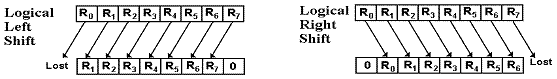
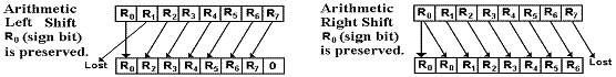
Register Shift Operations
We now discuss a number of shift operations performed on registers.
Mnemonic Description Type Format
SLA Shift left algebraic RS
SRA Shift right algebraic RS SRA R1,D2(B2)
SLL Shift left logical RS SLL R1,D2(B2)
SRL Shift right logical RS SRL R1,D2(B2)
SLDA Shift left double algebraic RS SLDA R1,D2(B2)
SRDA Shift left double algebraic RS SRDA R1,D2(B2)
SLDL Shift left double logical RS SLDL R1,D2(B2)
SRDL Shift right double logical RS SRDL R1,D2(B2)
The algebraic shifts preserve the sign bit in a register, and thus are useful for arithmetic.
The logical shifts do not preserve the sign bit.
The shift operations set the standard condition codes, for use by BC and BCR.
The
register numbers for the double shift instructions must be an even number,
referencing the first of an even–odd register pair (see below).
Shift Instructions: Object Code Format
All shift instructions are four–byte instructions of the form OP R1,R3,D2(B2).
|
Type |
Bytes |
|
1 |
2 |
3 |
4 |
|
RS |
4 |
R1,R3,D2(B2) |
OP |
R1
R3 |
B2
D2 |
D2D2 |
The first byte contains the 8–bit instruction code.
The
second byte contains two 4–bit fields, each of which encodes a register number.
The first register number (R1) is the register to be shifted. The second register number
(R3) is not used and conventionally set to 0.
The
third and fourth bytes contain a 4–bit register number and 12–bit value. In many
type RS instructions, these would indicate a base register and a displacement
to be
used to specify the memory address for the operand in storage.
For
the shift instructions, this field is considered as a value to indicate the
shift count.
The value is in the form below. B is the
number of the register to be used as a base
for the value. The next three
hexadecimal digits are added to the value in that register.
|
B D1 |
D2 D3 |
The sum is used as a shift count, not as an address. The two conventional uses are to specify a constant shift count and to use a register to contain the shift count. Consider the following two examples, each of which uses the SRA instruction with opcode X‘8A’.
Object
Code Source Code
8A
90 00 0A SRA 9,10 BASE REGISTER = 0, DISPLACEMENT
= 10; THE
SHIFT COUNT IS 10.
8A
90 B0 00 SRA 9,0(11) HERE REGISTER 11
(X‘B’) CONTAINS
THE SHIFT
COUNT.
Example Object Code Analysis: SLL
Shift Left Logical Operation code = X‘89’
This
is also a type RS instruction, though the appearance of a typical use seems to
deny
this. Consider the following instruction
which shifts R6 left by 12 bits.
SLL R6, 12 Again, I assume we have set R6 EQU 6
The above would be assembled as 89 60 00 0C, as decimal 12 is X‘C’.
The deceptive part concerns the value 12, used for the shift count. Where is that stored?
The answer is that it is not stored, but is used as a value for the shift count.
The
object code 00 0C literally
indicates the computation of a value that is an sum of
decimal 12 from the value in base register 0.
But “0” indicates that no base register is
used, hence the value for the shift is decimal 12.
Here are three lines from a working program I wrote on 2/23/2009.
000014 5840 C302 00308
47 L R4,=F’1’
000018 8940 0001 00001
48 SLL R4,1
00001C 8940 0002 00002
49 SLL R4,2
Note
that the load instruction makes use of a literal. The assembler will create an entry in the
literal pool and populate it with the value 1.
Here, my code calls for register 12 (X‘C’) to serve as
the base register. The literal is stored
at offset X‘302’
from the address stored
in that base register.
While it might seem plausible that the SLL instructions similarly generate literals, this is not the case. In each, as noted above, the value is stored as a count in the base/displacement format, which is here pressed into duty to store a value and not an address.
Single Shifts: Algebraic and Logical
Here
are some diagrams describing shifts in a single register. These examples will
assume an 8–bit register with the IBM bit numbering scheme; 32 bits are hard to
draw.
This figure illustrates logical shifts by 1 for these imaginary 8–bit registers.
This figure illustrates algebraic shifts by 1 for these imaginary 8–bit registers.
The
actual IBM assembler shift instructions operate on 32–bit registers and can
shift by
any number of bit positions. For single
register shifts, the shift count should
be a
non–negative integer less than 32. For
double register shifts, the upper limit is 63.
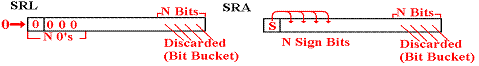
Double Register Shifts
Each of these four instructions operates on an even–odd register pair.
The algebraic shifts preserve the sign bit of the even register; the logical shifts do not.
Here is a diagram illustrating a double algebraic right shift.
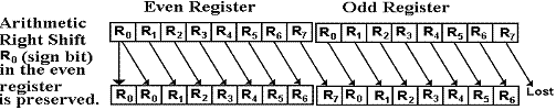
If
the above example were a logical double right shift, a 0 would have been
inserted into the leftmost bit of the even register.
Remember to consider the shifts in register pairs, preferably even–odd pairs.
Consider the following code: SR R9,R9 This clears R9
SRDL R8,32
The
double–register right shift moves the contents of R8 into R9 and clears R8,
as it is a logical shift.
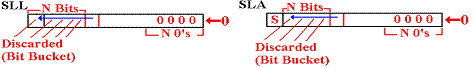
Single Register Left Shifts: Another View
First
consider the left shifts. There are two
single–register variants: SLL and
For
an N–bit logical left shift, bits 0 through (N – 1) are shifted out of the
register
and discarded. Bits 31 through (32 – N)
are filled with 0.
Bit 0 is not considered as a sign bit in a logical shift; it may change values.
For
an N–bit arithmetic left shift, bits 1 through N are shifted out of the
register
and discarded. Bits 31 through (32 – N)
are filled with 0. Bit 0 (the sign bit)
is not changed.
The
overflow bit can be set by an arithmetic left shift. This will occur if
the bit shifted out does not match the sign bit that is retained in bit 0.
We
shall see later that setting the overflow bit indicates that the result of the
shift cannot be viewed as a valid result of an arithmetic operation.
Single Register Right Shifts: Another View
Now consider the left shifts. There are two single–register variants: SRL and SRA.
For
either of these shift types, a shift by N bit will cause the N least
significant bits
to be shifted out of the register and discarded.
For
an N–bit logical right shift, the value 0 is shifted into the N most
significant bits,
bits 0 through (N – 1) of the register.
Bit 0 is not considered a sign bit and is
shifted into bit N of the register. The
sign of the number may change.
For
an N–bit arithmetic right shift, bit 0 is considered as a sign bit. Bit 0 is not changed,
but is shifted into bits 1 through N of the register. At the end, the (N + 1) most
significant bits of the register contain what used to be bit 0 (the sign bit).
For
an arithmetic right shift, the sign of the shifted result is the same as that
of the
original. If the sign bit originally is
0, the SRL and SRA produce identical results.
Double Register Shifts: Another View
The double register shifts are just generalizations of the single register shifts.
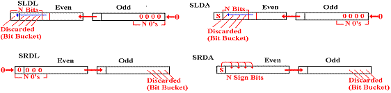
In these double register shifts, a pair of registers is viewed as a single 64–bit value.
The
IBM coding convention (and possibly the CPU hardware) calls for this pair to be
what is called an even–odd pair, in
which the odd number is one more than the even.
Examples of even–odd register pairs are: 4 and 5, 6 and 7, 8 and 9, 10 and 11.
Consider
the two registers R5 and R6. While it is
true that 5 is an odd number
and 6 is an even number; these two registers do not form an even–odd pair.
Each of these is a member of a distinct even–odd pair.
Shift Examples
Here are some typical shift examples, with comments.
SRA
R9,2 Algebraic right shift by 2 bit positions, equivalent to
division
by 4. SRA by N bit positions is equivalent to
division by 2N.
SLA R8,3 Algebraic
left shift by 3 bit positions, equivalent to multiplication
by 8.
NOTE: Multiplication using the M, MH, or MR instructions is rather slow, as is
division with
either D or DR. It is almost universal
practice to use
arithmetic left
shifts to replace multiplication by a power of 2 and
arithmetic
right shifts to replace division by a power of 2.
Example: Consider the following three lines of code.
L R5,AVAL ASSUME AVAL IS THE LABEL FOR A FULL-WORD
LR R6,R5 COPY VALUE INTO R6
SRA R6,3 SAME AS MULTIPLY BY 8
AR R6,R5 R6 NOW HAS 9 TIMES THE VALUE IN R5.
More on Shifting and Arithmetic
The
association of arithmetic left shifting with multiplication, and arithmetic
right
shifting with division is useful.
However, there are limits to this interpretation.
To
illustrate this for multiplication, I select an integer that is a simple power
of 2,
4096 = 212. As a 16–bit
integer, this would be stored in memory as follows.
|
Sign |
214 |
213 |
212 |
211 |
210 |
29 |
28 |
27 |
26 |
25 |
24 |
23 |
22 |
21 |
20 |
|
0 |
0 |
0 |
1 |
0 |
0 |
0 |
0 |
0 |
0 |
0 |
0 |
0 |
0 |
0 |
0 |
Taking the two’s complement of the above, we find that –4096 is stored as follows.
|
Sign |
214 |
213 |
212 |
211 |
210 |
29 |
28 |
27 |
26 |
25 |
24 |
23 |
22 |
21 |
20 |
|
1 |
1 |
1 |
1 |
0 |
0 |
0 |
0 |
0 |
0 |
0 |
0 |
0 |
0 |
0 |
0 |
We shall use each of these two
integer values to illustrate the limits of the arithmetic
left shift. We shall then consider the
following pair as subject to an arithmetic right shift.
+32 = 25 is stored as follows.
|
Sign |
214 |
213 |
212 |
211 |
210 |
29 |
28 |
27 |
26 |
25 |
24 |
23 |
22 |
21 |
20 |
|
0 |
0 |
0 |
0 |
0 |
0 |
0 |
0 |
0 |
0 |
1 |
0 |
0 |
0 |
0 |
0 |
–32 is stored as follows.
|
Sign |
214 |
213 |
212 |
211 |
210 |
29 |
28 |
27 |
26 |
25 |
24 |
23 |
22 |
21 |
20 |
|
1 |
1 |
1 |
1 |
1 |
1 |
1 |
1 |
1 |
1 |
1 |
0 |
0 |
0 |
0 |
0 |
Arithmetic Left Shifts as Multiplication
We
first consider some left shifts that can validly be interpreted as
multiplication.
For each of these integers, consider a
According
to our interpretation, a
The 4096 = 212 becomes 16384 = 214. This is as it should be.
4096·4 = 16384 and 212·22 = 214.
|
Sign |
214 |
213 |
212 |
211 |
210 |
29 |
28 |
27 |
26 |
25 |
24 |
23 |
22 |
21 |
20 |
|
0 |
1 |
0 |
0 |
0 |
0 |
0 |
0 |
0 |
0 |
0 |
0 |
0 |
0 |
0 |
0 |
The –4096 = –(212) becomes –16384 = –(214). This is as it should be.
(–4096)·4 = –16384 and –(212)·22 = –(214).
|
Sign |
214 |
213 |
212 |
211 |
210 |
29 |
28 |
27 |
26 |
25 |
24 |
23 |
22 |
21 |
20 |
|
1 |
1 |
0 |
0 |
0 |
0 |
0 |
0 |
0 |
0 |
0 |
0 |
0 |
0 |
0 |
0 |
Overflow on Shifting Left (Multiplication)
Consider again 4096 = 212, stored as a 16–bit integer.
|
Sign |
214 |
213 |
212 |
211 |
210 |
29 |
28 |
27 |
26 |
25 |
24 |
23 |
22 |
21 |
20 |
|
0 |
0 |
0 |
1 |
0 |
0 |
0 |
0 |
0 |
0 |
0 |
0 |
0 |
0 |
0 |
0 |
Consider the result of
According
to our interpretation, a
We note that 4096·8
= 32768 and 212·23 = 215 = 32768.
But,
the 4096 = 212 becomes –32768 = –(215). The sign has “gone bad”, as a result of
arithmetic overflow.
|
Sign |
214 |
213 |
212 |
211 |
210 |
29 |
28 |
27 |
26 |
25 |
24 |
23 |
22 |
21 |
20 |
|
1 |
0 |
0 |
0 |
0 |
0 |
0 |
0 |
0 |
0 |
0 |
0 |
0 |
0 |
0 |
0 |
But consider the same operation on –4096 = –(212).
|
Sign |
214 |
213 |
212 |
211 |
210 |
29 |
28 |
27 |
26 |
25 |
24 |
23 |
22 |
21 |
20 |
|
1 |
1 |
1 |
1 |
0 |
0 |
0 |
0 |
0 |
0 |
0 |
0 |
0 |
0 |
0 |
0 |
After the shift, we have the proper result; –4096·8 = –32768.
|
Sign |
214 |
213 |
212 |
211 |
210 |
29 |
28 |
27 |
26 |
25 |
24 |
23 |
22 |
21 |
20 |
|
1 |
0 |
0 |
0 |
0 |
0 |
0 |
0 |
0 |
0 |
0 |
0 |
0 |
0 |
0 |
0 |
More on Overflow While Shifting Left
In
this illustration we continue to focus on 16–bit two’s complement
integers.
A 32–bit representation would show the same problem, only at larger values.
Suppose we have the valid integer –32,768 = –(215). This is stored as follows.
|
Sign |
214 |
213 |
212 |
211 |
210 |
29 |
28 |
27 |
26 |
25 |
24 |
23 |
22 |
21 |
20 |
|
1 |
0 |
0 |
0 |
0 |
0 |
0 |
0 |
0 |
0 |
0 |
0 |
0 |
0 |
0 |
0 |
Suppose we attempt a
The result will remain the same. The
sign bit is always preserved in an arithmetic shift.
In
attempting a
(–32,768)·2 = –32,768.
(–32,768)·4 = –32,768.
(–32,768)·8 = –32,768.
In
other words, once overflow has been hit,
Arithmetic Right Sifting as Division
Here the results are a bit less strange. First consider our positive number, +32.
|
Sign |
214 |
213 |
212 |
211 |
210 |
29 |
28 |
27 |
26 |
25 |
24 |
23 |
22 |
21 |
20 |
|
0 |
0 |
0 |
0 |
0 |
0 |
0 |
0 |
0 |
0 |
1 |
0 |
0 |
0 |
0 |
0 |
A SRA 4 (Arithmetic Right Shift by 4) should yield 32/16 = 2. It does.
|
Sign |
214 |
213 |
212 |
211 |
210 |
29 |
28 |
27 |
26 |
25 |
24 |
23 |
22 |
21 |
20 |
|
0 |
0 |
0 |
0 |
0 |
0 |
0 |
0 |
0 |
0 |
0 |
0 |
0 |
0 |
1 |
0 |
Further shifting this result by 1 bit position will give the value 1 (as expected).
|
Sign |
214 |
213 |
212 |
211 |
210 |
29 |
28 |
27 |
26 |
25 |
24 |
23 |
22 |
21 |
20 |
|
0 |
0 |
0 |
0 |
0 |
0 |
0 |
0 |
0 |
0 |
0 |
0 |
0 |
0 |
0 |
1 |
However, any more SRA (Arithmetic Right Shifts) will give the value 0.
|
Sign |
214 |
213 |
212 |
211 |
210 |
29 |
28 |
27 |
26 |
25 |
24 |
23 |
22 |
21 |
20 |
|
0 |
0 |
0 |
0 |
0 |
0 |
0 |
0 |
0 |
0 |
0 |
0 |
0 |
0 |
0 |
0 |
This is as expected for integer division, and is not surprising.
More on Arithmetic Right Sifting as Division
Here the results are a bit less strange. Now consider our negative number, –32.
|
Sign |
214 |
213 |
212 |
211 |
210 |
29 |
28 |
27 |
26 |
25 |
24 |
23 |
22 |
21 |
20 |
|
1 |
1 |
1 |
1 |
1 |
1 |
1 |
1 |
1 |
1 |
1 |
0 |
0 |
0 |
0 |
0 |
A SRA 3 (Arithmetic Right Shift by 3) should yield (–32)/8 = (–4). It does.
|
Sign |
214 |
213 |
212 |
211 |
210 |
29 |
28 |
27 |
26 |
25 |
24 |
23 |
22 |
21 |
20 |
|
1 |
1 |
1 |
1 |
1 |
1 |
1 |
1 |
1 |
1 |
1 |
1 |
1 |
1 |
0 |
0 |
A SRA 2 (Arithmetic Right Shift by 2) should yield (–4)/4 = (–1). It does.
|
Sign |
214 |
213 |
212 |
211 |
210 |
29 |
28 |
27 |
26 |
25 |
24 |
23 |
22 |
21 |
20 |
|
1 |
1 |
1 |
1 |
1 |
1 |
1 |
1 |
1 |
1 |
1 |
1 |
1 |
1 |
1 |
1 |
But note that further Arithmetic Right Shifts continue to produce the result –1.
What we are saying is that (–1) / 2 = –1. If the above is acceptable, then the SRA works well as a substitution for division by a power of two.
Register Pairs: Multiplication and Division
We
now discuss two instructions that, in their full–word variants, demand the use
of a
64–bit “double word”. Rather than use
the type, we use a pair of registers.
The assembly language definition calls for “even–odd register pairs”.
Each pair of registers is referenced by its (lower numbered) even register.
The standard pairs from the general–purpose registers that are not reserved for other use are shown in the following list.
R4 and R5 R8 and R9
R6 and R7 R10 and R11
When
such a pair is referenced by a multiply or divide instruction, it is treated as
a 64–bit two’s–complement integer with the sign in bit 0 of the even register.
Remember
that the bits of a register are numbered left to right, so that bit 0 is
the sign bit and bit 31 is the rightmost (least significant) bit.
Examples: M R4,F2 MULTIPLY VALUE IN R5 BY VALUE IN
FULL-WORD
F2. RESULTS IN (R4, R5)
D R6,F3 DIVIDE 64-BIT NUMBER IN (R6, R7) BY F3
Full–Word Multiplication
This
slide will cover the two multiplication instructions based on full words.
The half–word multiplication instruction will be discussed later.
The two instructions of interest here are:
Mnemonic Description Type Format
M Multiply full–word RX M R1,D2(X2,B2)
MR Multiply register RR MR R1,R2
For
each of these, one uses a selected even–odd pair to hold the 64–bit product.
Here is the status of the registers in the selected pair; think (4, 5) or (8,
9), etc.
|
|
Even Register |
Odd Register |
|
Before multiplication |
Not used: contents are ignored |
Multiplicand |
|
After multiplication |
Product: high–order 32 bits |
Product: low–order 32 bits |
If the product can be represented
as a 32–bit number, the even register will contain
the extended sign bit, so that the 64–bit number in the register pair has the
right sign.
Note that the multiplication overwrites the value of the multiplicand in the odd register.
Full–Word Multiplication: Examples
In the first fragment, the starting value in R4 is irrelevant, as it is ignored.
Each example assumes two full–words: MULTCAND and MULTPLER.
L R5,MULTCAND LOAD THE MULTIPLICAND INTO R5.
SR R4,R4 CLEAR R4. THIS IS REALY USELESS.
M
R4,MULTPLER MULTIPLY BY A
FULLWORD
* R4 NOW HAS BITS 0 – 31 OF THE 64-BIT PRODUCT
* R5 NOW HAS BITS 32 – 63 OF THE 64-BIT
PRODUCT
Another code fragment:
L R9,MULTCAND LOAD THE MULTIPLICAND INTO R9.
L R5,MULTPLER LOAD MULTIPLIER INTO R5
MR R8,R5 MULTIPLY BY FULL-WORD VALUE IN R5
* R8 NOW HAS BITS 0 – 31 OF THE 64-BIT PRODUCT
* R9 NOW HAS BITS 32 – 63 OF THE 64-BIT
PRODUCT
Half–Word Multiplication
Mnemonic Description Type Format
MH Multiply half–word RX MH R1,D2(X2,B2)
This
instruction requires only one register.
It is loaded with the multiplicand before the
multiplication, and receives the product.
Note
that this is the product of a 32–bit number (in the register) and a 16–bit
number
in the half–word in memory. This will
result in a 48–bit product.
Of
bits 0 – 47 of the product, only bits 16 – 47 are retained and kept in the
32–bit
register as the product. If the absolute
value of the product is greater than 231, the sign
bit of the result (as found in the register) might not be the actual sign of
the product.
Here is an example of a proper use of the instruction, which will give correct results.
LH
R3,MULTCAND Each of
these two arguments is a half–word
MH
R3,MULTPLER with
value in the range: –215 £ N £ (215 – 1).
MULTCAND
DC H‘222’
MULTPLER
DC H‘44’
The magnitude of the product will not exceed (215)·(215) = 230, an easy fit for a register.
Full–Word Division
This
slide will cover the two division instructions based on full words.
The half–word division instruction will be discussed later.
The two instructions of interest here are:
Mnemonic Description Type Format
D Divide full–word RX D R1,D2(X2,B2)
DR Divide register RR DR R1,R2
For each of these, one uses a selected even–odd pair to hold the 64–bit dividend.
Here is the status of the registers in the selected pair; think (4, 5) or (8, 9), etc.
|
|
Even Register |
Odd Register |
|
Before division |
Dividend: high–order 32 bits |
Dividend: low–order 32 bits |
|
After division |
Remainder from division |
Quotient from division |
In each of the full–word division
operations, it is important to initialize the even register
of the pair correctly. There are two
cases to consider.
1. The dividend is a full 64–bit number, possibly loaded with a LM instruction.
2. The dividend is a 32–bit number. In that case, we need to initialize both registers.
Full–Word Division: Example 1
In
this example, I am assuming a full 64–bit dividend that is stored in two
adjacent
full words in memory. I use this memory
structure to avoid adding anything new.
LM R10,R11, DIVHI LOAD TWO FULLWORDS
D
R10,DIVSR NOW DIVIDE
* R10 CONTAINS THE REMAINDER
* R11 CONTAINS THE QUOTIENT
DIVHI DC F‘1111’
ARBITRARY NUMBER THAT IS NOT TOO BIG
DIVLO DC F‘0003’
ANOTHER ARBITRARY NUMBER
DIVSR DC F‘19’
THE DIVISOR
Important
Note: This process of assembling a
64–bit dividend from two full words
might
run into problems if DIVLO is seen
as negative.
Here, I choose to ignore that point.
Full–Word Division: Example 2
In
this example, I am assuming a 32–bit dividend and using a more standard
approach. Please note that it works only
for positive dividends.
SR
R10,R10 SET R10 TO 0
L
R11,DIVIDEND LOAD FULL–WORD
DIVIDEND
D
R10,DIVISOR DO THE DIVIDING
* R10 CONTAINS THE REMAINDER
* R11 CONTAINS THE QUOTIENT
DIVIDEND
DC F‘812303 JUST SOME NUMBER.
DIVISOR DC F‘16384’
A POWER OF TWO, SEE NOTE BELOW
NOTES: 1. This
works only for a positive dividend. The
reason is that, by clearing
the even
register of the even–odd pair, I have declared the 64–bit dividend
to be a
positive number, even if R11 is loaded with a negative number.
2. There is a much faster way to divide any number by a power
of two.
This method,
using a shift instruction, will be discussed later.
Full–Word Division: Example 3
In
this example, I am assuming a 32–bit dividend and using the standard approach
that will work correctly for all dividends.
The dividend is first loaded into the even
register of the even–odd pair and then shifted into the odd register.
This shifting causes the sign bit of the 64–bit dividend to be set correctly.
L
R10,DIVIDEND LOAD INTO THE EVEN
REGISTER
SRDA R10,32 SHIFTING BY 32 BITS PLACES
* THE DIVIDEND INTO R11.
* R10 RETAINS THE
SIGN BIT D R10,DIVISOR DO THE DIVIDING
* R10 CONTAINS THE REMAINDER
* R11 CONTAINS THE QUOTIENT
DIVIDEND
DC F‘812303 JUST SOME NUMBER.
DIVISOR DC F‘16384’
A POWER OF TWO, SEE NOTE BELOW
We shall discuss this a bit more after we have discussed the shift operations.
Full–Word Division: Example 4
Here is a more realistic example of the use of a full 64–bit dividend.
Code fragment 1: Create the 64–bit product and store in adjacent full words.
L
R5,MCAND LOAD THE
MULTIPLICAND INTO R5.
M
R4,MPLER MULTIPLY BY A
FULLWORD
* R4 NOW HAS BITS 0 – 31 OF THE 64-BIT PRODUCT
* R5 NOW HAS BITS 32 – 63 OF THE 64-BIT
PRODUCT STM R4,R5,PRODHI STORE THE
64-BIT PRODUCT
Code fragment 2: Some time later use the 64–bit product as a dividend for division.
LM
R10,R11,PRODHI LOAD TWO FULLWORDS
D
R10,DIVSR NOW DIVIDE
* R10 CONTAINS THE REMAINDER
* R11 CONTAINS THE QUOTIENT
PRODHI DC F‘0’
TWO FULL WORDS SET ASIDE
PRODLO DC F‘0’
64 BITS (8 BYTES) OF STORAGE.
Diversion: Shifting the Dividend into Place
Consider two possible dividends: + 100 and – 100.
Consider the code fragment below.
LH R6,=H‘100’
SRDA
R6,32
After the first instruction is executed, register R6 contains the full–word value +100, as shown below.
|
0 – 3 |
4 – 7 |
8 – 11 |
12 – 15 |
16 – 19 |
20 – 23 |
24 – 27 |
28 – 31 |
|
0000 |
0000 |
0000 |
0000 |
0000 |
0000 |
0110 |
0100 |
After the shift in the second
instruction, the contents of R6 have been shifted to R7,
leaving only the sign bit in R6.
R6
|
0 – 3 |
4 – 7 |
8 – 11 |
12 – 15 |
16 – 19 |
20 – 23 |
24 – 27 |
28 – 31 |
|
0000 |
0000 |
0000 |
0000 |
0000 |
0000 |
0000 |
0000 |
R7
|
0 – 3 |
4 – 7 |
8 – 11 |
12 – 15 |
16 – 19 |
20 – 23 |
24 – 27 |
28 – 31 |
|
0000 |
0000 |
0000 |
0000 |
0000 |
0000 |
0110 |
0100 |
Shifting the Dividend Into Place (Part 2)
Now consider the code fragment.
LH R8,=H‘-100’
SRDA
R8,32
After
the first instruction is executed, register R8 contains the full–word value
–100,
as shown below.
|
0 – 3 |
4 – 7 |
8 – 11 |
12 – 15 |
16 – 19 |
20 – 23 |
24 – 27 |
28 – 31 |
|
1111 |
1111 |
1111 |
1111 |
1111 |
1111 |
1001 |
1100 |
After the shift in the second
instruction, the contents of R8 have been shifted to R9,
leaving only the sign bit in R8.
R8
|
0 – 3 |
4 – 7 |
8 – 11 |
12 – 15 |
16 – 19 |
20 – 23 |
24 – 27 |
28 – 31 |
|
1111 |
1111 |
1111 |
1111 |
1111 |
1111 |
1111 |
1111 |
R9
|
0 – 3 |
4 – 7 |
8 – 11 |
12 – 15 |
16 – 19 |
20 – 23 |
24 – 27 |
28 – 31 |
|
1111 |
1111 |
1111 |
1111 |
1111 |
1111 |
1001 |
1100 |
Boolean Operators: AND, OR, XOR
We now conclude our investigation of binary integer data by examining the Boolean operators, which treat binary data one bit at a time. We shall repeat the basic definitions, discuss the implementation by IBM, and close by repeating a natural application. The three Boolean operators directly supported by IBM are the logical AND, OR, and NOT.
Each of these operates on binary data, one bit at a time according to the following tables.
AND 0·0 = 0 OR 0+0 = 0 XOR 0Å0 = 0
0·1 = 0 0+1 = 1 0Å1 = 1
1·0 = 0 1+0 = 1 1Å0 = 1
1·1 = 1 1+1 = 1 1Å1 = 0
To
show the bitwise nature of these operations, we consider a few examples as
applied to four–bit integers.
1010 1010 0101 0101 0101
· 0111 · 1101 + 0000 + 1111 Å 1111
0010 1010 0101 1111 1010
Note
that the XOR function can be used to generate the Boolean not function. The Boolean NOT, denoted by ![]() and defined by
and defined by ![]() . As seen above, this can be extended bitwise,
so that the rightmost example takes the logical NOT of the digits 0101.
. As seen above, this can be extended bitwise,
so that the rightmost example takes the logical NOT of the digits 0101.
One of the more
natural uses of the Boolean operators is to do bitwise operations on data
represented in 8–bit bytes and denoted by two 4–bit hexadecimal digits. There are three operations that will commonly
be seen in assembly language programs.
1. Select a bit position in a byte and force that bit to have the value 1.
2. Select a bit position in a byte and force that bit to have the value 0.
3. Select a bit position in a byte and flip the value of that bit.
We
shall examine the use of these operations on 4–bit fields, as longer data
structures
can be analyzed one hexadecimal digit at a time. We use the IBM bit numbering.
|
Bit number |
0 |
1 |
2 |
3 |
|
Bit value |
8 |
4 |
2 |
1 |
Here are the basic masking operations that can be performed on a 4–bit hexadecimal digit.
|
Bits Affected |
To set the bit, use OR with |
To clear the bit, use AND with |
||
|
None |
0000 |
X‘0’ |
1111 |
X‘F’ |
|
0 |
1000 |
X‘8’ |
0111 |
X‘7’ |
|
1 |
0100 |
X‘4’ |
1011 |
X‘B’ |
|
2 |
0010 |
X‘2’ |
1101 |
X‘D’ |
|
3 |
0001 |
X‘1’ |
1110 |
X‘E’ |
|
0 and 1 |
1100 |
X‘C’ |
0011 |
X‘3’ |
|
0 and 2 |
1010 |
X‘A’ |
0101 |
X‘5’ |
|
0 and 3 |
1001 |
X‘9’ |
0110 |
X‘6’ |
|
1 and 2 |
0110 |
X‘6’ |
1001 |
X‘9’ |
|
1 and 3 |
0101 |
X‘5’ |
1010 |
X‘A’ |
|
2 and 3 |
0011 |
X‘3’ |
1100 |
X‘C’ |
|
0, 1, and 2 |
1110 |
X‘E’ |
0001 |
X‘1’ |
|
0, 1, and 3 |
1101 |
X‘D’ |
0010 |
X‘2’ |
|
0, 2, and 3 |
1011 |
X‘B’ |
0100 |
X‘4’ |
|
1, 2, and 3 |
0111 |
X‘7’ |
1000 |
X‘8’ |
|
ALL |
1111 |
X‘F’ |
0000 |
X‘0’ |
System/370 architecture supports three Boolean functions, each in four formats.
|
Instruction |
Format |
Operands |
||
|
Logical AND |
Logical OR |
Logical XOR |
|
|
|
NR |
OR |
XR |
RR |
Two registers |
|
N |
O |
X |
RX |
Register and storage |
|
NI |
OI |
XI |
SI |
Register and immediate |
|
NC |
OC |
XC |
SS |
Two storage locations |
Each of these twelve instructions sets the condition codes used by the conditional branch instructions in the same way. If every bit in the result is 0, the result is 0 and condition code 0 is set. If any bit in the result is 1, the result is not negative and condition code 1 is set, as if the result were negative. Here are two equivalent ways to test results.
To determine Yes No
All target bits are 0 Use BZ Use BNZ
Any target bit is 1 Use BM Use BNM
Here are the logical instructions, grouped by type.
Type
RR
This is a two–byte instruction of the form OP R1,R2.
|
Type |
Bytes |
Operands |
|
|
|
RR |
2 |
R1,R2 |
OP |
R1 R2 |
The first byte contains the 8–bit instruction code. The second byte contains two 4–bit fields, each of which encodes a register number. This instruction format is used to process data between registers.
Here are the three Boolean instructions of this type.
NR Logical AND Opcode is X‘14’
OR Logical OR Opcode is X‘16’
XR Logical Exclusive OR Opcode is X‘17’
Type
RX
This is a four–byte instruction of the form OP R1,D2(X2,B2).
|
Type |
Bytes |
Operands |
1 |
2 |
3 |
4 |
|
RX |
4 |
R1,D2(X2,B2) |
OP |
R1 X2 |
B2 D2 |
D2D2 |
The first byte contains the 8–bit instruction code. The second byte contains two 4–bit fields, each of which encodes a register number. The first operand, encoded as R1, is the target register for the instruction. The second register number, encoded as X2, is the optional index register. Bytes 3 and 4 together contain the address of the second operand in base and displacement form, which may be modified by indexing if the index register field is not zero.
Here are the three Boolean instructions of this type.
N Logical AND Opcode is X‘54’
O Logical OR Opcode is X‘56’
X Logical Exclusive OR Opcode is X‘57’
Type
SI
This is a four–byte instruction of the form OP D1(B1),I2.
|
Type |
Bytes |
Operands |
1 |
2 |
3 |
4 |
|
SI |
4 |
D1(B1), I2 |
OP |
I2 |
B1 D1 |
D1D1 |
The first byte contains the 8–bit instruction code. The second byte contains the 8–bit value of the second operand, which is treated as an immediate operand. The instruction contains the value of the operand, not its address. The first operand is an address, specified in standard base register and displacement form. Note that this first operand must reference the address of a single byte, as this is a byte–oriented operation.
Here are the three Boolean instructions of this type.
NI Logical AND Opcode is X‘94’
OI Logical OR Opcode is X‘96’
XI Logical Exclusive OR Opcode is X‘97’
Type
SS
These are of the form OP D1(L,B1),D2(B2), which provide a length for only operand 1. The length is specified as an 8–bit byte.
|
Type |
Bytes |
Operands |
1 |
2 |
3 |
4 |
5 |
6 |
|
SS(1) |
6 |
D1(L,B1),D2(B2) |
OP |
L |
B1
D1 |
D1D1 |
B2
D2 |
D2D2 |
The first byte contains the operation code. The second byte contains a value storing one less than the length of the first operand, which is the destination for the operation.
Bytes 3 and 4 specify the address of the first operand, using the standard base register and displacement format. Bytes 5 and 6 specify the address of the second operand, using the standard base register and displacement format.
Here are the three Boolean instructions of this type.
NC Logical AND Opcode is X‘D4’
OC Logical OR Opcode is X‘D6’
XC Logical Exclusive OR Opcode is X‘D7’
Another Look at Case Conversion
In order to investigate the difference between upper case and lower case letters, we here present a slightly different version of the EBCDIC table. Admittedly, we have covered this in a previous chapter, but cover it again within the context of the Boolean operators.
|
|
Zone |
8 |
C |
9 |
D |
A |
E |
|
Numeric |
|
|
|
|
|
|
|
|
1 |
|
“a” |
“A” |
“j” |
“J” |
|
|
|
2 |
|
“b” |
“B” |
“k” |
“K” |
“s” |
“S” |
|
3 |
|
“c” |
“C” |
“l” |
“L” |
“t” |
“T” |
|
4 |
|
“d” |
“D” |
“m” |
“M” |
“u” |
“U” |
|
5 |
|
“e” |
“E” |
“n” |
“N” |
“v” |
“V” |
|
6 |
|
“f” |
“F” |
“o” |
“O” |
“w” |
“W” |
|
7 |
|
“g” |
“G” |
“p” |
“P” |
“x” |
“X” |
|
8 |
|
“h” |
“H” |
“q” |
“Q” |
“y” |
“Y” |
|
9 |
|
“i” |
“I” |
“r” |
“R” |
“z” |
“Z” |
The structure implicit in the above
table will become more obvious when we compare
the binary forms of the hexadecimal digits used for the zone part of the code.
Upper
Case C = 1100 D = 1101
E = 1110
Lower Case 8 = 1000 9 = 1001
A = 1010
Note that
it is only one bit in the zone that differentiates upper case from lower case.
In binary, this would be noted as 0100 or X‘4’. As this will operate on the zone field of a
character field, we extend this to the two hexadecimal digits X‘40’. The student should verify that the
one’s–complement of this value is X‘BF’. Consider the following operations.
UPPER CASE
‘A’ X’1100
0001’ X’1100
0001’
OR X ‘40’ X‘0100 0000’ AND X ‘BF’ X‘1011 1111’
X’1100 0001’ X’1000 0001’
Converted to ‘A’ ‘a’
Lower case
‘a’ X’1000
0001’ X’1000
0001’
OR X ‘40’ X‘0100 0000’ AND X ‘BF’ X‘1011 1111’
X’1100 0001’ X’1000 0001’
Converted to ‘A’ ‘a’
We now
have a general method for changing the case of a character, if need be.
Assume that the character is in a one byte field at address LETTER.
Convert a character to upper
case. OI,LETTER,=X‘40’
This leaves upper case characters unchanged.
Convert a character to lower
case. NI,LETTER,=X‘BF’
This leaves lower case characters unchanged.
Change
the case of the character. XI,LETTER,=X‘40’
This changes upper case to lower case and lower case to upper case.