The above example assumes decimal (base 10) notation, which is the notation most commonly used by humans for representing integers. In our studies of digital computers, we must consider not only decimal numbers but also binary (base 2), octal (base 8) and hexadecimal (base 16). It is conventional to represent the base of every number system as a decimal number. Any other approach would lead to considerable confusion.
In a positional number system, the value of a string of digits is expressed in terms of powers of the base B. Consider the four-digit number, denoted in the abstract as D3D2D1D0. The value of this number is given by D3·B3 + D2·B2 + D1·B1 + D0·B0. For example, consider the number 1101. The value of this number depends on the base of the number system.
In decimal notation, we have 1·103 + 1·102 + 0·101 + 1·100 = 1·1000 + 1·100 + 0·10 + 1·1 = 1000 + 100 +1 = 110110.
In octal numbers (base 8), we have
11018 = 1·83 + 1·82
+ 0·81
+ 1·80
= 1·512 +
1·64
+ 0·8
+ 1·1 = 57710.
In hexadecimal numbers (base 16), we have
110116 = 1·163 + 1·162 + 0·161
+ 1·160
= 1·4096
+ 1·256
+ 0·16
+ 1·1 = 445310.
In binary numbers (base 2), we have
11012 = 1·23 + 1·22
+ 0·21
+ 1·20
= 1·8 + 1·4 + 0·2 + 1·1 = 1310.
Common examples of encoders and decoders are based on either two–bit or three–bit arithmetic. Two bits can encode four numbers, 0 through 3 in unsigned binary. Three bits can encode eight numbers, 0 through 7 in unsigned binary. In general, N bits can encode 2N different numbers, 0 through 2N – 1 in unsigned binary.
Binary Decimal
The
two-bit codes are 00 0
01 1
10 2
11 3
The
three-bit codes are 000 0
001 1
010 2
011 3
100 4
101 5
110 6
111 7
Multiplexers and Demultiplexers
A multiplexer has a
number of inputs (usually a power of two), a number of control signals, and one
output. A demultiplexer has one input
signal, a number of control signals, and a number of outputs, also usually a
power of two. We consider here a 2N–to–1
multiplexer and a 1–to–2N demultiplexer.
Circuit Inputs Control Signals Outputs
Multiplexer 2N N 1
Demultiplexer 1 N 2N
The action of each
of these circuits is determined by the control signals. For a multiplexer, the output is the selected
input. In a demultiplexer, the input is
routed to the selected output. As
examples, we show the diagrams for both a four–to–one multiplexer (MUX) and a
one–to–four demultiplexer (DEMUX).
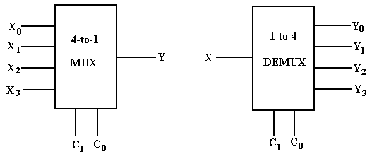
Note that each of
the circuits has two control signals.
For a multiplexer, the N control signals select which of the 2N
inputs will be passed to the output. For
a demultiplexer, the N control signals select which of the 2N
outputs will be connected to the input.
Multiplexers
The output for a
multiplexer can be represented as a Boolean function of the inputs and the
control signals. As an example, we
consider a 4-input multiplexer, with control signals labeled C0 and
C1 and inputs labeled I0, I1, I2,
and I3. The output can be
described as a truth table or algebraically.
Note that each of the truth tables and algebraic expression shows the
input that is passed to the output. The
truth table is an abbreviated form of the full version, which as a table for
independent variables C0, C1, I0, I1,
I2, and I3 would have 64 rows.
C1 C0 M
0 0 I0
0 1 I1 M = C1’·C0’·I0 +
C1’·C0·I1 + C1·C0’·I2 +
C1·C0·I3
1 0 I2
1 1 I3
Multiplexers are generally described as 2N–to–1 devices. These multiplexers have 2N inputs, one of which is connected to the single output line. The N control lines determine which of the inputs is connected to the output. Here is a circuit for a 4–to–1 multiplexer. Note that the inputs are labeled X3, X2, X1, and X0 here and I3, I2, I1, and I0 in the multiplexer equation.
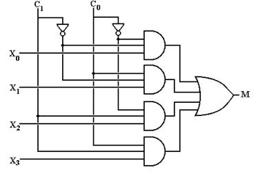
Demultiplexer
Demultiplexers are generally described as 1–to–2N devices. These multiplexers have one input, which is connected to one of the 2N output lines. The N control lines determine which of the output line is connected to the input. Here is a circuit for a 1–to–4 demultiplexer, which might be called “active high” in that the outputs not selected are all set to 0. Note that multiplexers do not have the problem of unselected outputs; a MUX has only one output.
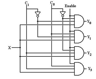
Note that, for good measure, we have added an enable–high to the demultiplexer. When this enable is 0, all outputs are 0. When this enable is 1, the selected output gets the input, X. Remember, that X can have a value of either 0 or 1.
We shall return to
demultiplexers after we have discussed decoders. At that time, we shall note a similarity
between the decoders and demultiplexers, consider the use of a decoder as a demultiplexer,
and investigate the possibility of an active–low demultiplexer.
We close our
discussion of multiplexers and demultiplexers with the two theorems.
Theorem 1: Any Boolean function of N Boolean variables,
N > 0, can be constructed by
a multiplexer with
2N inputs and N control lines, labeled CN-1 … C0.
Proof: We give as a proof a method for constructing
the function. We then give an
example. The method is as follows:
1. Connect the N variables to the N
control lines CN-1 … C0.
It is generally easier
to connect the control lines
in order of the variables listed; thus for F(X, Y, Z) we
would connect X to C2,
Y to C1, and Z to C0.
This is merely a convenience.
2. Write the multiplexer equation in terms
of the input variables; thus for F(X, Y, Z),
we write the multiplexer
equation as

3. Write the Boolean function in Canonical
Sum of Products form. If the variables
have been properly associated
with the control lines, the terms in the Canonical
SOP should be in the same
order as the terms in the multiplexer equation.
4. Match the function F(X, Y, Z) to the
multiplexer. If a product term appears
in
the Boolean function, set the
input to 1. Otherwise set the input to
0.
Example: Consider the function F2 = X·Y + X·Z + Y·Z, which we have
identified as the carry-out of a full adder with inputs X, Y, and Z.
We begin by
connecting the variables to control lines in the suggested order. Connect X to C2, Y to C1,
and Z to C0; thus C2 = X, C1 = Y, and C0
= Z.
Writing the
multiplexer equation in terms of the input variables, we get:

We now write the
Boolean function in Canonical Sum of Products form.

In the S–list form we
say F2 = S(3, 5, 6,
7).
The final step is to
assign the inputs:
I0 = 0 I1 = 0 I2 = 0 I3 = 1
I4 = 0 I5 = 1 I6 = 1 I7 = 1.
We now show the design, again using X0 through X7 as labels for inputs.
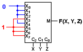
This figure suggests a simpler way to design with multiplexers using this theorem.
1) Force the expression
into a canonical SOP expression.
2) Write
the canonical SOP expression as a S list
3) Connect
the multiplexer inputs corresponding to numbers in the list to 1.
4) Connect
the other inputs to 0.
Above, the design shows the
implementation of F(X, Y, Z) = S(3,
5, 6, 7). Note that inputs
3, 5, 6, and 7 are connected to logic 1; the others are connected to logic 0.
There are also two ways to implement an expression in POS. For each method we force the expression into canonical POS. We can then do one of two things: convert to canonical SOP and implement as above, or use the POS list as a list of inputs to set to 0; thus
1) Connect the
multiplexer inputs corresponding to numbers in the P list to 0.
2) Connect
the other inputs to 1.
Above, the design shows the implementation of the same function F(X, Y, Z) = S(3, 5, 6, 7), now called F(X, Y, Z) = P(0, 1, 2, 4). Note that inputs 0, 1, 2, and 4 are connected to logic 1; the others are connected to logic 0.
We close the discussion of this theorem with a remark on logical complexity as opposed to physical complexity. The logical complexity of a circuit is most readily expressed in the number of logic gates in the circuit. An alternate measure would be the maximum number of gates between any input and the output; this would determine the time delay of the circuit.
What might
be called the “physical complexity” of a circuit is best measured in the number
of physical chips that we use. Consider
our function F1(X, Y, Z) = S(1,
2, 4, 7). As we shall see later, direct
implementation with basic gates requires three NOT gates, four 3–input AND
gates, and a 4–input OR gate. This
requires four chips: one 6–input NOT chip, two triple
3–input AND chips and one double 4–input OR chip.
As we shall see below, this may be fabricated from a 3–to–8 decoder and one double 4–input OR chip, for a total of two chips. We have just seen the fabrication with a 8–to–1 multiplexer, a total of one chip. Physically, the last design is the simplest.
For all of these designs we assume that the control inputs have been set in the correct order.
We now consider another way to
design with multiplexers. This method is
a bit more complex, and thus should be used less often. In this author’s view, it is less important.
However, your author cannot resist the impulse to impart knowledge, so here it
is.
Theorem 2: Any Boolean function of (N + 1) Boolean
variables, N > 0, can be constructed
by a multiplexer
with 2N inputs and N control lines.
Proof: We give as a proof a method for constructing
the function. We then give an example. The method is as follows:
1. Connect any N variables to the control
lines. This leaves one variable
unconnected.
2. Express the Boolean function in normal
SOP form. Each term must have a literal
for
each of the N variables that
are connected to the control lines and may contain the
other one. Put another way, each of the 2N
product terms possible on the N variables
attached to the control lines
must be included in a term in this expression.
3. Connect the remaining variable, its
complement, 0, or 1 to the 2N input lines.
4. Match the terms.
Example:
Consider the
function F2 = A·B + A·C + B·C, which we have identified as the carry-out
of a full adder with inputs A, B, and C.
Arbitrarily, we connect A and B to the control lines.
This implies that
each of the terms in F2 must contain both A and B, either in complemented or
plain form. To get this, we use some
algebra to expand the last two terms.
F2 = A·B + A·C + B·C
= A·B + A·(B + B’)·C + (A + A’)·B·C
= A·B + A·B·C + A·B’·C + A·B·C + A’·B·C
= A·B + A·B·C + A·B·C + A·B’·C + A’·B·C
= A·B + A·B·C + A·B’·C + A’·B·C as X + X = X
= A·B·(1 + C) + A·B’·C + A’·B·C
= A·B + A·B’·C + A’·B·C as 1 + C = 1
for all C.
Note that the form
produced is not canonical as the first term is lacking a C. It is, however, in the required sum of
products form. To complete the
construction, we rewrite F2 and match it against the multiplexer equation for a
4-input multiplexer.
F2 =
A’·B’·0 + A’·B·C +
A·B’·C + A·B·1
M =
C1’·C0’·I0 +
C1’·C0· +
C1·C0’·I2 + C1·C0·I3
The match-up is C1
= A, C0 = B, I0 = 0, I1 = C, I2 =
C, and I3 =1.
With these inputs,
the multiplexer has synthesized the function F2.
Decoders and Encoders
We now consider an
important class of commercial circuits – encoders and decoders. These perform the functions suggested by the
corresponding decimal-binary conversions.
In conversion of a decimal number to binary, we obtain the binary
equivalent of the number. An encoder has
a number of inputs, usually a power of two, and a set of outputs giving the
binary code for the “number” of the input.
Encoders
Consider a classic 2N–to–N
encoder. The inputs are labeled I0,
I1, …, IK, where K = 2N – 1. The assumption is that only one of the inputs
is active; in our way of thinking only one of the inputs is 1 and the rest are
0. Suppose input J is 1 and the rest are
0. The output of the circuit is the
binary code for J. Suppose a 32–to–5
encoder with input 18 active. The output
Z is the binary code 10010; Z4 = 1, Z3 = 0, Z2
= 0, Z1 = 1, and Z0 = 0.
Common encoders
include 8–to–3, 16–to–4, and 32–to–5.
One common exception to the rule of 2N–to–N is a 10–to–4
encoder, which is used because decimal numbers are so common. Note that three binary bits are not
sufficient to encode ten numbers, so we must use four bits and not produce the
outputs 1010, 1011, 1100, 1101, 1110, or 1111.
We now present a detailed discussion and a design of a 10-to-4 encoder. We begin with a diagram that might illustrate a possible use of an encoder.
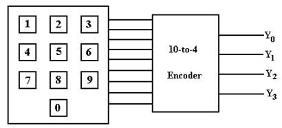
In this example, the key pad has ten keys, one for each digit. When a key is pressed, the output line corresponding to that key goes to logic 1 (5 volts) and the other output lines stay at logic 0 (0 volts). Note that there are ten output lines from the key pad, one for each of the keys. These ten output lines form ten input lines into the 10–to–4 encoder.
The 10–to–4 encoder outputs a binary code indicating which of the keys has been pressed. In a complete design, we would require some way to indicate that no key has been pressed. For our discussion, it is sufficient to ignore this common case and assume that a key is active.
We first ask why we need four bits for the encoder. N bits will encode 2N different inputs. As a result, to encode M different items, we need N bits with 2N–1 < M £ 2N. To encode 10 inputs, we note that 23 < 10 £ 24, so we need 4 bits to encode 10 items.
We now present a table indicating the output of the encoder for each input. In this example, we assume that at any time exactly one input is active.
|
Input |
Y3 |
Y2 |
Y1 |
Y0 |
|
X0 |
0 |
0 |
0 |
0 |
|
X1 |
0 |
0 |
0 |
1 |
|
X2 |
0 |
0 |
1 |
0 |
|
X3 |
0 |
0 |
1 |
1 |
|
X4 |
0 |
1 |
0 |
0 |
|
X5 |
0 |
1 |
0 |
1 |
|
X6 |
0 |
1 |
1 |
0 |
|
X7 |
0 |
1 |
1 |
1 |
|
X8 |
1 |
0 |
0 |
0 |
|
X9 |
1 |
0 |
0 |
1 |
In the table at left, we label the inputs X0 through X9, inclusive. To produce the equations for the outputs, we reason as follows.
Y3 is 1 when either X8 = 1 or X9 = 1.
Y2 is 1 when X4 = 1 or X5 = 1 or X6 = 1 or X7 = 1.
Y1 is 1 when X2 = 1, X3 = 1, X6 = 1, or X7 = 1.
Y0 is 1 when X1 = 1, X3 = 1, X5 = 1, X7 = 1, or X9 = 1.
These observations lead to the following equations, used to design the encoder.
Y3
= X8 + X9
Y2 = X4
+ X5 + X6 + X7
Y1 = X2
+ X3 + X6 + X7
Y0 = X1
+ X3 + X5 + X7 + X9
Here is the circuit for the 10-to-4 encoder.
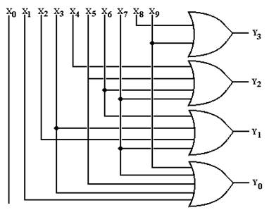
The student will note that input X0 is not connected to an output. This gives rise to the following problem for the circuit: how does one differentiate between X0 being active and no input being active. That might be a problem for real encoder design.
The most straightforward modification of the circuit would be to create the logical OR of the ten inputs and pass that signal as a “key pressed” signal. We mention this only to show that some applications must handle this case; we shall not consider it further in this course.
Another issue with encoders
is what to do if two or more inputs are active. For ‘plain” encoders the output is not
always correct; for example, in the above circuit with inputs X3 and
X5 active would output Y3 = 0, Y2 = 1, Y1
= 1, and Y0 = 1.
Priority encoders
are designed to avoid the problem of multiple inputs by implementing a priority
order on the inputs and producing the output for the input that has priority.
For example, in a 32-to-5 priority encoder, having inputs 18 and 29 active
would produce either the binary code 10010 (for 18) or 11101 (for 29),
depending on the priority policy, and not the output 11111 that a plain encoder
would produce.
Decoders
An N–to–2N
decoder does just the opposite, taking an N bit binary code and activating the
output labeled with the corresponding number.
Consider a 4–to–16 decoder with outputs labeled Z0, Z1,
…, Z15. Suppose the input is
I3 = 1, I2 = 0, I1 = 0, and I0 = 1
for the binary code 1001. Then output Z9
is active and the other outputs are not active.
Again, the main
exception to the N–to–2N rule for decoders is the 4–to–10 decoder,
which is a common circuit. Note that it
takes 4 bits to encode 10 items, as 3 bits will encode only 8. This author’s preference would be to use a 4–to–16
decoder and ignore some of the outputs, but this author does not establish
commercial practice. The main advantage
is that the
4–to–10 decoder chip would have 6 fewer pins than a 4–to–16 decoder; a 16–pin
chip is standard and cheaper to manufacture than a 22–pin chip.
Another issue is
whether the signals are active high or active low. Our examples have been constructed for active
high circuits. Consider the 4–to–16
decoder as an example. If the input code
is 1001, then the output Z9 is a logic 1 (+5 volts) and all other
outputs are logic 0
(0 volts). This approach is active
high. In real commercial circuits, we
often have outputs as active low, in which case the above decoder would have
output Z9 as a logic 0 (0 volts) and all other inputs as logic 1 (+5
volts). This reflects an issue with
design using real TTL circuits or with standard circuit emulators, such as
MultiSim or Multi–Media Logic.
Decoders have N inputs and 2N outputs. We consider a 3–to–8 decoder; thus N = 3. The design that we present will assume that the decoder is active high; again that the selected output becomes logic 1 (5 volts) and the others remain at logic 0 (ground or 0 volts).
|
Decimal |
Binary |
|
0 |
000 |
|
1 |
001 |
|
2 |
010 |
|
3 |
011 |
|
4 |
100 |
|
5 |
101 |
|
6 |
110 |
|
7 |
111 |
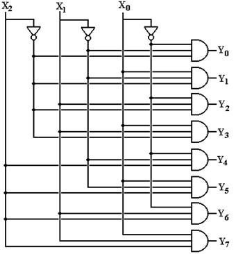
The decoder is based on the association of binary numbers to decimal numbers, as is shown in the figure at right. Since this is a 3–to–8 decoder, we have three inputs, labeled X2, X1, and X0; and eight outputs, labeled Y7, Y6, Y5, Y4, Y3, Y2, Y1, and Y0.
The observation that leads to the design of the decoder is the obvious one that the values of X2, X1, and X0 determine the output selected. For this part of the discussion, I choose to ignore the enable input.
We introduce the Enable output in a later discussion.
The following Boolean equations determine the 3–to–8 decoder.
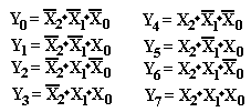
Here is the circuit diagram for the 3–to–8 active–high decoder.
The Enable Input
We now consider
another important input to the decoder chip.
This is the enable input. If the
decoder enable signal is active high, then the decoder is active when enable is
1 and not active when enable = 0. We
shall consider enabled-high decoders here.
The enable input allows the decoder to be either enabled or disabled. For an active high decoder that is enabled high (Enable = 1 activates it) we have the following.
Enable = 0 All outputs of the decoder are 0
Enable = 1 The selected output of the decoder is 1,
all other outputs are 0.
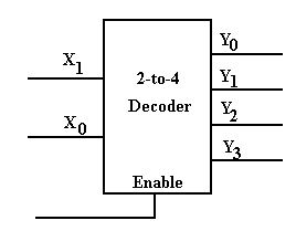 One way to express the effect of the enable
input is to use a modified truth table.
Enable X1 X0 Y0 Y1 Y2 Y3
0
d d 0
0 0 0
1
0 0 1
0 0 0
1
0 1 0
1 0 0
1
1 0 0
0 1 0
1
1 1 0
0 0 1
Thus, all outputs
are 0 when the enable input is 0. This
is true without regard to the inputs.
When the enable input is 1, the outputs correspond to the inputs.
Here is a circuit diagram for a 2–to–4 decoder that is enabled high and active high.
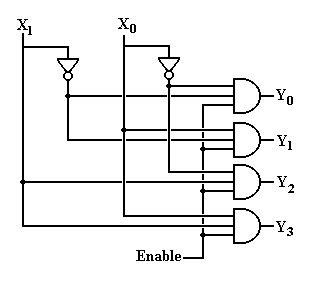
Note that the Enable input is passed as an input to all four of the AND gates used to produce the output of the decoder. As a result, when Enable = 0, all of the outputs are 0; the decoder is not active.
When Enable = 1 in the above circuit, the other two inputs X1 and X0 will determine the one of the four outputs is set to 1; the others remaining 0. This is exactly how the active-high decoder should function.
The following
example illustrates the use of the enable input for decoders. We use two
two-to-four decoders to construct a single three-to-eight decoder. The way to do this is to use one of the
inputs, conventionally the high-order bit, as an enable signal. This way one of the two-to-four decoders will
be enabled and one will not be. Here is
the circuit.
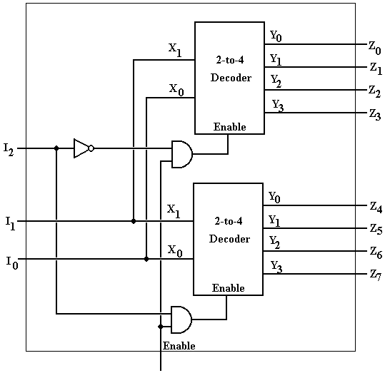
Suppose the three-to-eight
decoder is enabled. Under this
assumption, the input I2 selects the two–to–four decoder that is
active. It I2 = 0, then the
top decoder is active and the bottom decoder is not active (all its outputs are
0). It I2 = 1, then the
bottom decoder is active and the top decoder is not active (all its outputs are
0). In either case, the inputs I1
and I0 are passed to both two-to-four decoders.
When I2 = 0, the inputs I1 and I0 select
which of outputs Y0, Y1, Y2, or Y3
in the top two-to-four decoder is active and thus which of Z0, Z1,
Z2, or Z3 is active.
When I2 =
1, the inputs I1 and I0 select which of outputs Y0,
Y1, Y2, or Y3 in the bottom two-to-four
decoder is active and thus which of Z4, Z5, Z6,
or Z7 is active. Thus we have
constructed the equivalent of a three-to-eight decoder.
The Active–Low,
Enabled–Low Decoder
We now examine a decoder designed according to standard commercial
practice. This decoder is active–low and
enabled–low.
The
enable input allows the decoder to be either enabled or disabled. For a decoder that is enabled low (Enable = 0
activates it) we have the following:
Enable = 1 None of the outputs of the decoder are active.
Enable = 0 Only the selected output is active; all others are inactive.
For a
decoder that is enabled–low and active–low, we have the following:
Enable = 1 All outputs are 1; no output is active.
Enable = 0 Only the selected output has value 0 (active);
all others
have value 1 (inactive).
One way to express
the effect of the enable input is to use a modified truth table. Here we examine a 2–to–4 decoder that is enabled–low
and active–low.
Enable X1 X0 Y0 Y1 Y2 Y3
1
d d 1
1 1 1
0
0 0 0
1 1 1
0
0 1 1
0 1 1
0
1 0 1
1 0 1
0
1 1 1
1 1 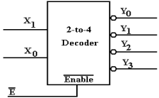
We may immediately
deduce the decoder equations
from the truth table just above. Here
they are.
![]()
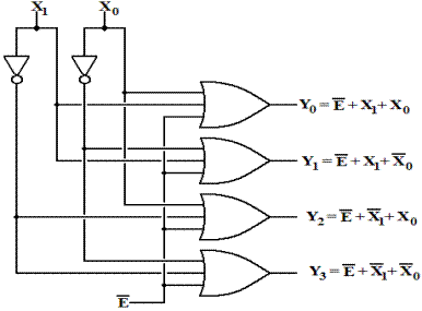
Here is the
circuit diagram for a 2–to–4 decoder that is active low and enabled low.
We now repeat an earlier design, this time with decoders that are
enabled–low. We use two
two–to–four decoders (active low and enabled low) to construct a single
three–to–eight decoder, that is also active low and enabled low. The way to do this is to use one of the
inputs, conventionally the high–order bit, as an enable signal. This way one of the 2–to–4 decoders will be
enabled and one will not be. Here is the
circuit.
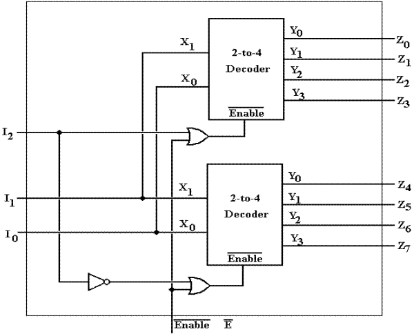
Suppose that the
3–to–8 decoder is disabled; ![]() = 1. Then, each of the 2–to–4 decoders is also
disabled and all outputs are logic 1.
This is as it should be.
= 1. Then, each of the 2–to–4 decoders is also
disabled and all outputs are logic 1.
This is as it should be.
Suppose the 3–to–8
decoder is disabled; ![]() = 0. Under this assumption, the input I2
selects the 2–to–4 decoder that is active.
It I2 = 0, then the top decoder is active (with its Enable
set to 0) and the bottom decoder is not active (with its Enable set to 1). It I2 = 1, then the bottom decoder
is active (its Enable = 0) and the top decoder is not active (its Enable = 1). In either case, the inputs I1 and
I0 are passed to both 2–to–4 decoders.
= 0. Under this assumption, the input I2
selects the 2–to–4 decoder that is active.
It I2 = 0, then the top decoder is active (with its Enable
set to 0) and the bottom decoder is not active (with its Enable set to 1). It I2 = 1, then the bottom decoder
is active (its Enable = 0) and the top decoder is not active (its Enable = 1). In either case, the inputs I1 and
I0 are passed to both 2–to–4 decoders.
When I2 = 0, the inputs I1 and I0 select
which of outputs Y0, Y1, Y2, or Y3
in the top 2–to–4 decoder is active and thus which of Z0, Z1,
Z2, or Z3 is active.
When I2 =
1, the inputs I1 and I0 select which of outputs Y0,
Y1, Y2, or Y3 in the bottom
2–to–4 decoder is active and thus which of Z4, Z5, Z6,
or Z7 is active. Thus we have
constructed the equivalent of a 3–to–8 decoder.
There is an equivalence between decoders and demultiplexers that many
students notice. Consider a 1–to–2N
demultiplexer with N control signals, under the assumption that the selected
output copies the input and the other outputs are set to the logic value
considered inactive. The demultiplexer
may be considered either as “active high”, with the inactive outputs set to
logic 0, or “active low”, with the inactive outputs set to logic 1
Consider the “active high” demultiplexer.
We then set the input (labeled “Enable” in the diagram) to logic 1 and
note that the output selected by the control signals is logic 1 while the other
outputs are logic 0. When the input
(“Enable”) is set to logic 0, all of the outputs are logic 0. We have converted the demultiplexer into an
active–high decoder.
The following figure shows a 1–to–4 demultiplexer used as a 2–to–4
decoder.
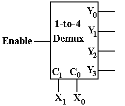
Note that the input
to the circuit acting as a decoder is labeled X1 and X0. This input is placed into the control inputs
of the demultiplexer, indicating which output should receive the input, set to
the decoder enable signal. When Enable =
0, all of the outputs are 0, as required for the decoder.
When Enable = 1, the X1 X0 input selects which
output becomes 1 while the other outputs remain at 0. This makes the DEMUX so
configured to be functionally equivalent to a 2–to–4 decoder.
We now note a confusing usage in commercial chips, as seen in the
Multi–Media Logic tool.
The following chips are labeled demultiplexers; the one on the left called a
2–to–4 DEMUX and the one on the right called a 3–to–8 DEMUX.
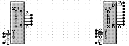
In reality, each of these is an active–low,
enabled–low decoder. In each, if ![]() = 1, all of the
outputs are logic 1. In each, if
= 1, all of the
outputs are logic 1. In each, if ![]() = 0, the
selected output is logic 0 and the rest are logic 1.
= 0, the
selected output is logic 0 and the rest are logic 1.
It is easy to see that each of the above may
be used as an “active low” demultiplexer.
Think of the ![]() input as input
to the demultiplexer. What we have is as
follows:
input as input
to the demultiplexer. What we have is as
follows:
If ![]() = 1, all
outputs are logic 1 (inactive).
= 1, all
outputs are logic 1 (inactive).
If ![]() = 0, the
selected output is logic 0 and the other outputs are logic 1.
= 0, the
selected output is logic 0 and the other outputs are logic 1.
In either case, the selected output has the value of the input.
Implementation of SOP expressions with decoders
We now consider the use of decoders as elements in a circuit. We first discuss active–high decoders for
this design, although they are rarely used in commercial circuits. For such encoders, the design calls for use
with OR gates to implement a function expressed in canonical SOP form.
We now give two
examples of circuit design with decoders.
Recall two functions specified
 by truth tables.
A B C F1 F2
0 0 0 0 0
0 0 1 1 0
0 1 0 1 0
0 1 1 0 1
1 0 0 1 0
1 0 1 0 1
1 1 0 0 1
1 1 1 1 1
We use an
active–high decoder to implement these two functions.
Each of the two functions is represented in the truth table in a way that
can easily be converted into canonical SOP form. F1 can be seen as the sum of canonical
product terms
1, 2, 4, and 7. F2 can be seen as the
sum of the canonical product terms 3, 5, 6, and 7. In the standard notation, we say F1 = S(1, 2, 4, 7) and F2 = S(3, 5, 6, 7).
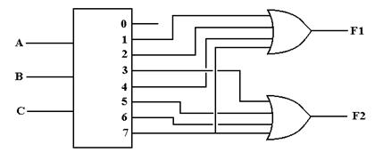
The circuit to the right of the truth table shows the use of an
active-high positive logic 3-to-8 decoder and an OR gate to synthesize each of
the functions F1 and F2. The method for
each function is the same. First
represent the function in the canonical SOP list form and then connect each of
the indicated outputs from the decoder to the OR gate for the function.
To synthesize F1 = S(1, 2, 4, 7) we connect the outputs 1, 2, 4,
and 7 from the decoder to the OR gate for F1.
The output of this OR gate is F1.
Basis of the Designs
The design above is quite straightforward.
Start with an active–high decoder and the S–list canonical
representation of the function. Attach
the outputs listed in the S–list to an OR gate.
Your author would like, at this moment, to develop the logical basis of
this strategy.
In the discussion below we shall consider design with both Active–High decoders and Active–Low decoders. It is hoped that this intuitive discussion will assist the reader to understand not only decoders themselves but also their use in the generation of arbitrary Boolean functions.
As always in our design
examples, we select a function that would better be implemented by a much
simpler circuit. The goal here is to
present the method, not develop a clever design. The function to be implemented is one of the
two that we have been discussing at some length in this and previous chapters: F2 = S(3, 5, 6, 7) = P(0, 1, 2, 4).
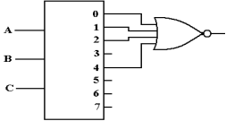
This function displays the unusual symmetry that there are 4 terms in both its SOP and POS expressions. All of our designs will use some sort of 4–input gate to combine the output of some sort of 3–to–8 decoder.
We begin by characterizing a number of basic gates. For the purpose of illustration, we examine 4–input gates. What is said is true for any number of inputs to these gates.
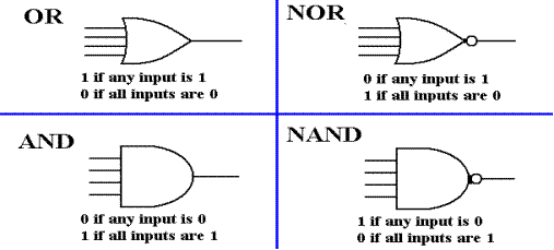
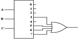
We now consider an active high decoder. For this and other examples, we assume that the decoder has been enabled; else all of its outputs are 0. An active high decoder outputs logic 1 for its selected output and logic 0 for the outputs not selected. For F2, we have:

Seeking a gate that outputs 1 if at least one of its inputs is 1, we are led to the OR gate.
Seeking a gate that outputs 1 only if all its inputs are 0, we are led to the NOR gate.
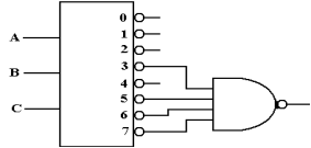
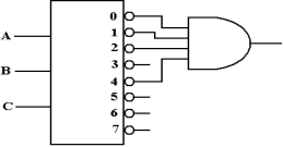
We now consider an active low decoder. For this and other examples, we assume that the decoder has been enabled; else all of its outputs are 1. An active high decoder outputs logic 0 for its selected output and logic 1 for the outputs not selected. For F2, we have:

Looking for a gate that outputs 0 if all of its inputs are logic 1 and outputs logic 1 if at least one of its inputs is logic 0, we find the NAND gate.
Looking for a gate that outputs 1 if and only if all of its inputs are 1, we find the AND gate.
Implementation of
POS Expressions with Decoders
We have a number of options, the first of which is the most common. Just convert the expression to Sum of Products and continue.
Thus, if we are given F2(A, B, C) = P(0, 1, 2, 4), we
just convert the expression to
F2(A, B, C) = S(3, 5, 6, 7) and continue with our work. Remember that the numbers in a canonical
expression on N variables run from (0 through 2N – 1). The number is in the
S–list if and only if it is not in the P–list. The discussions above actually indicate how
to construct the circuits directly from a canonical expression.
We note here that almost all commercially available decoders are
active–low. Those in our lab are
active–low. It is that fact that is one
of the reasons for this long discussion.
Design Summary: Decoder
Type and Expression
Active High, SOP Attach
the specified outputs as input to an OR gate.
Example: F2(A, B, C) = S(3, 5, 6, 7)

Active High, POS Attach the specified outputs as input to a
NOR gate
Example: F2(A, B, C) = P(0, 1, 2, 4)

Active Low, SOP Attach the specified outputs as input to
a NAND gate
Example: F2(A, B, C) = S(3, 5, 6, 7)

Active Low, POS Attach the specified outputs as input to
an AND gate.
Example: F2(A, B, C) = P(0, 1, 2, 4)

Interlude: More
Designs with Multi–Media Logic.
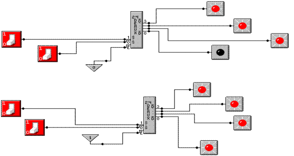
The first design shows two experiments with a 2–to–4 enabled–low,
active–low decoder, which Multi–Media Logic labels as a “2:4 DEMUX”. In the top figure, we have ![]() = 0 and the
selected output is set to logic 0 (seen by the LED being off). In the bottom figure, we have
= 0 and the
selected output is set to logic 0 (seen by the LED being off). In the bottom figure, we have ![]() = 1, and none
of the outputs are active. Each output
is logic 1, as seen by the corresponding LED being illuminated.
= 1, and none
of the outputs are active. Each output
is logic 1, as seen by the corresponding LED being illuminated.
Often, experiments such as this set are the only way to determine the
real behavior of a circuit element.
Here is an
implementation of our two functions F1 = P(0, 3, 5, 6) and F2 = P(0, 1, 2, 4)
that uses an active high 3–to–8 decoder and two 4–input AND gates.

As we shall see in the section immediately following, these two functions
(F1 and F2) have more common names that correspond to their standard usage in
computers.
Design of a Full Adder
We now investigate the design of a full adder. A full-adder is specified by its truth table.
|
A |
B |
C |
Sum |
Carry |
|
0 |
0 |
0 |
0 |
0 |
|
0 |
0 |
1 |
1 |
0 |
|
0 |
1 |
0 |
1 |
0 |
|
0 |
1 |
1 |
0 |
1 |
|
1 |
0 |
0 |
1 |
0 |
|
1 |
0 |
1 |
0 |
1 |
|
1 |
1 |
0 |
0 |
1 |
|
1 |
1 |
1 |
1 |
1 |
A full adder circuit adds two bits (A and B) with a carry-in C.
It produces two outputs the Sum and the Carry our to the next
higher stage. Here we elect to translate the truth table to two
Sum of Products expressions and implement the Sum and Carry
using AND-OR logic.
SUM = A’·B’·C + A’·B·C’ + A·B’·C’ + A·B·C
CARRY = A·B + A·C + B·C (this has been simplified).
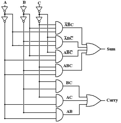
Here is one design of a Full-Adder using the basic Boolean gates.
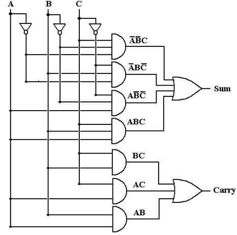
As an aside, we show a more conventional variant of the full adder circuit, one that is designed to address the “fan-out” problem. Consider the input labeled A in either circuit. It must be generated by another circuit element that is capable of delivering input to only a limited amount of gates. In the first circuit, the source of the signal A must drive five gates: the NOT gate producing A’ and the AND gates producing A·B’·C’, A·B·C, A·B, and A·C. The circuit below is a common variant in which each of the A, B, and C inputs is driving only one gate – the first NOT gate of the double inverter pair. Such a design provides for a standard input load for the circuit and facilitates its use in design.
Gate Delays and Timing Analyses
At this point, we move on to creating a “ripple carry” adder, which is a simple collection of a number of full adders to generate the sum of two multi-bit integers. In order to undertake this design, we must first do a rough timing analysis of the full adder.
Consider the three basic gates from which a full adder is built. We normally do not consider the time delay for producing the output, but consider the circuit only after all transients have disappeared. However, there are occasions upon which we must consider the fact that the output of a given logic gate does not change immediately with the input, but only after a short time delay, called the “gate delay”.
Each gate introduces a delay and produces its output only after the delay. This delay is unique to the gate type and method of manufacture; thus an AND gate would display a gate delay different from that of a NOT gate. For simplicity, we just assume that all gates have the same delay, normally in the range 1 – 5 nanoseconds. We may note that the gates used in commercial microprocessors are etched onto the CPU chip and have gate delays that are considerably less, probably on the order of 100 picoseconds (0.10 nanoseconds).
In order to explain, consider three basic gates, each of which has its input change at T = 0.

We begin our analysis at a time called T = – 1, and assume that the inputs have been stable for some time. At this time, the gate outputs are exactly what we expect.

At T = 0, the inputs to each gate suddenly change. Note that the outputs of the gates have not yet changed, as the change has yet to propagate through each gate.

At T = 1, by definition one gate delay after each input has changed, the outputs of each of the three gates finally reflects the changed inputs and the circuits again display the expected results. This is an example of the effect of gate delays – the changes in input gradually propagate through the circuit, with the output of a gate at T = K depending on its input at the previous time T = K – 1.
Before the Input Changes
We now consider a timing
analysis of the first version of the full adder (the one without the double not
gates). Suppose at T = 0, the input changes
from A = 0, B = 0, C = 0 to
A = 1, B = 0, C = 1. We begin at T = –
1, at which time the inputs have been stable for some time, so that all values
in the circuits follow what would be expected from the Boolean equations for
the SOP expressions of the Sum and Carry-Out.
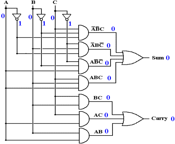
Figure: The Situation before Any Input
Change
The Input Changes
At T = 0 the input changes suddenly to A = 1, B = 0, C = 1. The situation is shown below. The new inputs are shown in RED, but note that none of the gate outputs (shown in BLUE) have yet changed. The change has not propagated through the gates and the circuit might be considered to be in a logically inconsistent state.
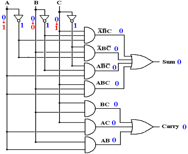
Figure:
The Circuit at T = 0, the Instance of Input Change
Author’s note: At this point, the only way to avoid confusion is to show both the previous value and current value of a changed input. The gate outputs, shown in blue, still depend on the old values and have not reacted to the new values.
After One Gate Delay
After one gate delay, the output of the gates that receive the input directly have changed, but the outputs of the gates one or more steps removed from the input have not changed. Again, the changed values are shown in RED, while the unchanged values are shown in BLUE. Note the notation OLD ® NEW, used in an attempt to avoid confusion in understanding the input to the AND gates, which are still responding to the status at T = 0.
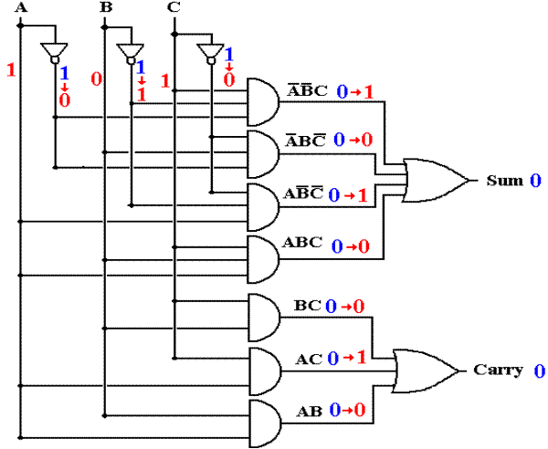
Figure: The Full Adder after One Gate Delay
Note the output of the top AND gate. At T = 0, the value of C has changed to 1, but the value of A’ and B’ are still 1, so we have A’ = 1, B’ = 1, and C = 1. The output of A’·B’·C at T = 1 depends on these values, which have changed from A’ = 1, B’ = 1, and C = 0; thus the value of A’·B’·C changes from 0 to 1. We note that the value will change again.
After Two Gate Delays, the Carry-Out is Correct
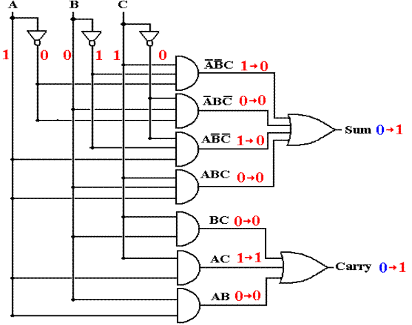
Figure: The Full Adder after Two Gate
Delays
After two gate delays, the effect of the input change has moved through all of the AND gates and the OR gate for the generation of the Carry-Out, which is now correct. Note that the SUM output has changed to 1, a result of the values of A’·B’·C and A·B’·C’ at T = 1.
After Three Gate Delays, the Output is Stable
After three gate delays, the output has changed to reflect the new input.
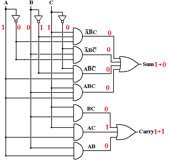
The progress of the change in the circuit is summarized in the table below.
|
T |
A |
B |
C |
A’ |
B’ |
C’ |
A’B’C |
A’BC’ |
AB’C’ |
ABC |
S |
AB |
AC |
BC |
CO |
|
-1 |
0 |
0 |
0 |
1 |
1 |
1 |
0 |
0 |
0 |
0 |
0 |
0 |
0 |
0 |
0 |
|
0 |
1 |
0 |
1 |
1 |
1 |
1 |
0 |
0 |
0 |
0 |
0 |
0 |
0 |
0 |
0 |
|
1 |
1 |
0 |
1 |
0 |
1 |
0 |
1 |
0 |
1 |
0 |
0 |
0 |
1 |
0 |
0 |
|
2 |
1 |
0 |
1 |
0 |
1 |
0 |
0 |
0 |
0 |
0 |
1 |
0 |
1 |
0 |
1 |
|
3 |
1 |
0 |
1 |
0 |
1 |
0 |
0 |
0 |
0 |
0 |
0 |
0 |
1 |
0 |
1 |
Ripple Carry Adders
The circuit above shows a full adder that takes two one-bit numbers and a one-bit carry-in and produces a one-bit sum and a one-bit carry-out. One bit adders might be cute, but our design will require a 32-bit adder/subtractor. Let’s extend this design.
The first step in the extension is to make a 32-bit ripple-carry adder. The significance of the term “ripple carry” will become obvious soon. The design of such an adder would be rather messy, so we here present a 4-bit ripple-carry adder. Such an adder is made from four full adders. The circuit, shown below, adds two four bit numbers A3A2A1A0 and B3B2B1B0.

A 32-bit ripple-carry adder will be made from 32 full adders. The name “ripple carry” arises from a timing analysis of the circuit, which we now undertake. Consider the first circuit showing a full adder. We count the number of gate levels required for each of the two outputs: we have two levels for the carry and three for the sum. The circuit shown has four full adders, labeled from right to left as FA0, FA1, FA2, and FA3. A 32-bit ripple carry adder would have 32 full adders, labeled from right to left as FA0 through FA31. Note that the input for full adder FAK is the triple AK, BK, and CK; its output is SK and CK+1. For 0 £ K £ 31, the output CK+1 from full adder FAK is an input to the next full adder FAK+1. It is this fact that gives rise to the name “ripple-carry” as full adder FAK+1 cannot produce a correct output until some time after full adder FAK has provided the correct value of CK+1 for use as input.
Note that FA0 has C0 º 0, as the carry-in input is grounded. This effectively reduces the full adder to a half adder. The reason for keeping FA0 as a full adder will become apparent soon.
Let FA0 be the
full adder taking in A0, B0, and C0 (C0
= 0) to produce the sum S0 and
carry-out C1. If all input is
at T = 0, FA0 produces C1 at T = 2 and S0 at T
= 3. But FA1 cannot produce
correct output until C1 is correctly set by FA0. Thus FA1 produces C2 at
T = 4 and S1 at T = 5. In
general, one can show the following.
Full adder FAK gets its input correct at time T = 2·K.
Full adder FAK produces a correct carry-out at time T = 2·K + 2.
Full adder FAK produces a correct sum at time T = 2·K +
3.
The correct answer “ripples” through the adder as the carry bits become
correct.
Before we develop the 32-bit ripple-carry adder/subtractor, we must note that no modern computer uses a ripple-carry adder, as such devices are far too slow. We are talking about producing a 32-bit sum after 65 gate delays, approximately 130 nanoseconds. Real adders use a trick called “carry-look-ahead” in which the carry into higher order adders is computed in a more complex, but much more time-efficient manner.
We now consider the
construction of a subtractor, again using a 4-bit unit for illustration. We use a feature of two’s-complement
arithmetic that mimics true arithmetic in that subtraction can be implemented
as addition of the negative: A – B = A + (– B).
But recall that negation in the two’s complement system is achieved by
taking the one’s-complement (bitwise logical NOT) and adding 1, so A – B = A + ![]() + 1. This suggests a design for a subtractor,
which we develop only for a single bit unit.
+ 1. This suggests a design for a subtractor,
which we develop only for a single bit unit.
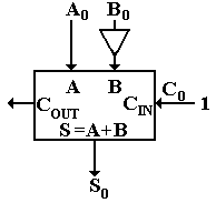
This is interesting, but we
want an adder/subtractor. Such a circuit
is achieved by recalling an interesting property of the XOR function: 0 Å B = B and 1 Å B = ![]() . This
observation allows us to design an adder/subtractor controlled by the signal
. This
observation allows us to design an adder/subtractor controlled by the signal ![]() .
.

When ![]() = 0, this
circuit adds the two 4-bit integers A and B.
When
= 0, this
circuit adds the two 4-bit integers A and B.
When ![]() = 1, this
subtracts the 4-bit integer B from the 4-bit integer A. Thus we have the desired circuit, which can
easily be extended to thirty two bits.
Again, a real adder/subtractor will be fabricated using look-ahead
technology, but the above circuit is logically correct.
= 1, this
subtracts the 4-bit integer B from the 4-bit integer A. Thus we have the desired circuit, which can
easily be extended to thirty two bits.
Again, a real adder/subtractor will be fabricated using look-ahead
technology, but the above circuit is logically correct.
Arithmetic Overflow – “Busting the Arithmetic”
We continue our examination of computer arithmetic to consider one more topic – overflow. Arithmetic overflow occurs under a number of cases:
1) when two positive numbers are added and
the result is negative
2) when two negative numbers are added and the result is
positive
3) when a shift operation changes the sign bit of the result.
In mathematics, the sum of two negative numbers is always negative and the sum of two positive numbers is always positive. The overflow problem is an artifact of the limits on the range of integers and real numbers as stored in computers. We shall consider only overflows arising from integer addition.
We consider only two’s-complement arithmetic. The textbook considers only 32-bit numbers, but we use 16-bit numbers as allowing simpler examples. For two’s-complement arithmetic, the range of storable integers is as follows:
16-bit – 215 to 215 – 1 or – 32768 to 32767
32-bit – 231 to 231 – 1 or – 2147483648 to 2147483647
The bits in an integer are numbered from left (most significant) to right (least significant), with the most significant bit having the highest number*. The bits are numbered 31 to 0 for 32-bit numbers, 15 to 0 for 16 bit numbers, and 7 to 0 for 8–bit numbers. In the standard integer notation, the most significant (left–most) bit is the sign bit; for 32–bit arithmetic bit 31 is the sign bit, and for 16–bit arithmetic the sign bit is bit 15.
Overflow in addition occurs when two numbers, each with a sign bit of 0, are added and the sum has a sign bit of 1 or when two numbers, each with a sign bit of 1, are added and the sum has a sign bit of 0. For simplicity, we consider 16–bit addition. As an example, consider the sum 24576 + 24576 in both decimal and binary. Note that 24576 = 16384 + 8192 = 214 + 213.
24576 0110 0000 0000 0000
24576 0110 0000 0000 0000
– 16384 1100 0000 0000 0000
Note that, as unsigned addition, the binary value is correct. However, in 16–bit arithmetic, bit 15 is the sign bit. We have two positive numbers (bit 15 is 0) giving rise to a negative sum (bit 15 is 1). This is an example of overflow.
In fact, 24576 + 24576 = 49152 = 32768 + 16384. The overflow is due to the fact that the number 49152 is too large to be represented as a 16-bit signed integer.
*NOTE: This is not the notation used by IBM for its mainframe and
enterprise computers.
In the IBM notation,
the most significant bit (often the sign bit) is bit 0 and the
least significant bit
has the highest number; bit 7 for an 8–bit integer.
Common Notation (8–bit entry) IBM Mainframe Notation
|
Bit # |
7 |
6 |
5 – 1 |
0 |
|
|
Sign |
MSB |
|
LSB |
|
Bit # |
0 |
1 |
2 – 6 |
7 |
|
|
Sign |
MSB |
|
LSB |
We now consider 16-bit addition. As inputs we have two 16-bit numbers A and B
A = A15A14A13A12A11A10A9A8A7A6A5A4A3A2A1A0
B = B15B14B13B12B11B10B9B8B7B6B5B4B3B2B1B0
For each number, bit 15 is the sign bit, bit 14 is the bit
for 214 = 16384, bit 13 is the bit for
213 = 8192, etc.
Conceptually, a 16-bit adder comprises sixteen one-bit full adders, each
taking in a carry bit from the lower order adder and producing both a sum bit
and a carry-out bit. The following
figure shows the three high order full adders for the three high order bits.
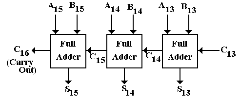
Overflow occurs in two cases
When A15 = 0, B15
= 0, and S15 = 1 Two
positive numbers sum to a negative number
When A15 = 1, B15
= 1, and S15 = 0 Two
negative numbers sum to a positive number
To understand overflow, we need only to consider the full-adder used to add the two sign bits; in this case we consider the full adder for bit 15.
|
A15 |
B15 |
C15 |
S15 |
C16 |
Overflow |
|
0 |
0 |
0 |
0 |
0 |
No |
|
0 |
0 |
1 |
1 |
0 |
YES |
|
0 |
1 |
0 |
1 |
0 |
Not possible |
|
0 |
1 |
1 |
0 |
1 |
Not possible |
|
1 |
0 |
0 |
1 |
0 |
Not possible |
|
1 |
0 |
1 |
0 |
1 |
Not possible |
|
1 |
1 |
0 |
0 |
1 |
YES |
|
1 |
1 |
1 |
1 |
1 |
No |
It is easy to prove that overflow is not possible when adding numbers of opposite signs. When adding two valid 16 bit numbers, overflow can occur only when the magnitude of the sum is greater than the magnitude of either of the two input numbers – this can occur only when the two numbers have the same sign. Consider the two rows A15 = 0, B15 = 0, C15 = 1, S15 = 1
and A15 = 1, B15 = 1, C15 = 0, S15 = 0.
These are the only two cases in which overflow occurs. Closer inspection of this full-adder table gives rise to a simpler method for identifying the overflow cases. Only in these two cases of overflow is C16 ¹ C15. For all other cases we have C16 = C15. So, our overflow detector is a circuit that detects when C16 ¹ C15. The Exclusive OR gate is exactly what we need; C16 Å C15 = 1 if and only if C16 ¹ C15. Thus, the signal is generated by
Overflow =
C16 Å
C15, or
Overflow = C32 Å C31
for 32 bit numbers.
Saturation Arithmetic
We now discuss a type of integer arithmetic in which overflow cannot occur. We consider 8-bit integers in both unsigned and two’s-complement form. The range of integers representable in 8-bits is as follows:
Unsigned integers 0 to 255
Two’s-Complement – 128 to
127
Saturation arithmetic is most commonly used in computer graphics, where color values may be conveniently represented as a RGB triple of 8-bit integers, one integer for each of the Red, Green, and Blue intensities of the color. In such a situation, we want the addition operator to saturate at its maximum value rather than overflow. This avoids some rather bizarre visual effects in the graphics display, such as the appearance of black spots in a white region.
The rule for saturation arithmetic is quite simple. If the value computed is not in the range representable for the data type, adjust it to the range by either setting it to the minimum or maximum value as appropriate.
Consider saturated 8-bit unsigned arithmetic. All results must be in the range [0, 255], that is – at least 0 and not greater than 255.
128 + 64 = 192 as in standard arithmetic
128 +
128 = 255 in standard arithmetic this overflows as 256 > 255.
in
saturation arithmetic this saturates at 255.
32 – 16 = 16 as in standard arithmetic
32 – 48 = 0 in standard arithmetic this causes an error.
The following table summarizes the difference between standard and saturation arithmetic.
Type of Arithmetic Result Greater Result Smaller
Than
Maximum Than Minimum
Number
Representable Number Representable
Standard Arithmetic Error Error
Saturation Arithmetic Set the result Set the result
to
the maximum to the
minimum
number representable number representable
Saturation
arithmetic is used mostly in graphics cards, also called “graphical processing
units”. The ALU designed for this text
will not provide for saturation arithmetic.
Multiplication and Division
Here we shall study circuits to perform integer multiplication and division. We shall spend some time considering circuits to perform these operations on unsigned positive integers, and then sketch out the design of realistic circuits that operate on integers in two’s–complement form. Due to the complexity of these circuits, they are not normally included in the ALU, but are placed in a related circuit called the MDU (Multiplication & Division Unit).
We note immediately that multiplication of two N–bit integers yields a product with 2N bits. For that reason, we shall discuss N–bit multiplication with a 2N–bit product, and N–bit division with a 2N–bit dividend, an N–bit divisor, an N–bit quotient, and N–bit remainder. This “doubling of the digits” is seen in decimal as well as binary multiplication.
Decimal: 9,999 · 9,999 = 99,980,001
Binary 1111 · 1111 = 1110 0001 (15
·
15 = 225)
The
computer designed for this course will yield a 64–bit product of two 32–bit
integers.
The division will call for a 64–bit dividend, with 32–bit divisors, quotient,
and remainder.
We begin with a consideration of multiplication for unsigned positive integers. At one level, this is quite simple, as the “times table” is very small. Here it is.
|
A |
B |
A·B |
|
0 |
0 |
0 |
|
0 |
1 |
0 |
|
1 |
0 |
0 |
|
1 |
1 |
1 |
One might note that this is exactly the truth table for the logical AND function, which is denoted by the same symbol as multiplication. This might suggest the use of the logical AND gate in a multiplier; the true circuits are even simpler. Consider a labeled example.
1011 the multiplicand, with
decimal value 11
1001 the multiplier, with
decimal value 9
1011
0000
0000 the four
partial products
1011___
1100011 the
product, with decimal value 99
Note that there are four partial products, one for each bit in the multiplier. Each partial product is the length of the multiplicand, and is either a copy of the multiplicand or all 0. The standard assumption is that the multiplicand and multiplier have equal length, each having the length of the standard integer in the architecture. All commercial designs allow different lengths for integer representations (8–bit, 16–bit, 32–bit, etc.), providing a number of distinct multiplication operations (8–bit by 8–bit, 16–bit by–16 bit).
This textbook will focus on two distinct integer sizes: 4–bit unsigned integers to introduce the basic ideas of multiplication and division, and 32–bit signed two’s–complement integers for the MDU as used in the design implemented in later chapters.
The above
example is based on human experience with multiplication. A straightforward
implementation would require four temporary registers, one for each of the
partial products. As we shall quickly
see, this is not necessary.
Consider the following problem, first solved in the traditional way with a slight change.
1011 Multiplicand = decimal 11
0111 Multiplier = decimal 7
1011 This is decimal
11
10110 This is 2·11 = decimal 22
101100 This is 4·11 = decimal 44
0000000
01001101 64 + 8 + 4 + 1 = 77
Modern multiplication algorithms are based on shifting and adding. This allows one to use the minimum number of registers required to hold the operands and the results.
For this
example, label the multiplier bits as M3M2M1M0;
M3 = 0, M2 = 1, M1 = 1, M0 =
1.
For 4–bit multiplication, we initialize the register set used for the product
to eight 0’s.
At
the start, the situation is as follows. Multiplicand 1011
Results 00000000
M0
= 1, add multiplicand to results Multiplicand 1011
Results 00001011
Shift
the results register set right Multiplicand 1011
Results 00001011
M1
= 1, add multiplicand to results Multiplicand 1011
Results 00100001
Shift
the results register set right Multiplicand 1011
Results 00100001
M2
= 1, add multiplicand to results Multiplicand 1011
Results 01001101
Shift
the results register set right Multiplicand 1011
Results 01001101
M3
= 0, do not add. Multiplicand 1011
Results 01001101
For the
more general discussion of the algorithm and its implementation in hardware, we
use
the register names from the Multiply/Divide Unit that will be the prototype for
that used in
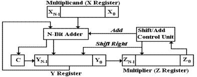
the computer we shall design. There are
three registers: X, Y, and Z.
At the
beginning: X contains the
multiplicand and Z contains the multiplier.
Y is
initialized to all zeroes.
At the end The register pair (Y, Z)
contains the product.
Register
X is not altered.
For this
chapter, each of the three registers will be assumed to have four bits. In the design
discussed later, each will be a 32–bit register. The example used will be the multiplication
of
1011 (decimal 11) by 1101 (decimal 13) to get the product 1000 1111 (decimal
143).
Here is the basic circuit diagram for the multiplier.
Here is the
formal algorithm.
1. Initialize C = 0, Y = 0, X =
multiplicand, Z = multiplier, Count = N.
2. At each step, examine Z0.
If Z0 = 1, then add X and
Y to put the sum in Y and set the carry bit C.
3. Right shift the register pair (Y, Z), with C ® YN-1 and Y0 ® ZN-1. Z0 is lost.
4. Decrement the count. If count = 0, stop. If not, go to step 2.
We now illustrate the algorithm with the example specified just above.
At the
start of the multiplication, the registers are initialized as follows:
X = 1011, Y = 0000, Z = 1101, and C = 0.

Z0 = 1, so there is an addition.

Then there is a right shift.

Now Z0 = 0, so there is no addition. The next step is another right shift.

Z0 = 1, so there is an addition.
1011
0010
01101
Here, the Y register gets the 4–bit sum 1101, and the carry bit is set to C = 0.

Then, there is the third
right shift.

Z0 = 1, so there is an addition.
1011
0110
10001
Here, the Y register gets the 4–bit sum 0001, and the carry bit is set to C = 1.

The final shift gives the product 1000 1111 (decimal 143) in the (Y, Z) register pair.

One of the advantages of
two’s–complement arithmetic is that such numbers can be handled as unsigned
integers for the purpose of addition and subtraction. Unfortunately, the unsigned
multiplication algorithm will not work for multiplication of signed
integers. The algorithm most commonly
implemented for two’s–complement multiplication is called Booth’s algorithm, developed by Andrew Donald Booth of Birkbeck
College in London England in 1951. We
shall not cover that algorithm in this text.
Division
Division is a bit more complex than multiplication, but is based on a similar algorithm. We shall study division for unsigned binary numbers, using one of the simpler, hence less efficient, algorithms. As before, this algorithm is based on manual practice.
Multiplication
was cast in the form of two arguments, each of N bits in length, producing
a product that was 2N bits in length.
Division will be defined for N–bit unsigned integers as follows: the
dividend has 2N bits, the divisor has N bits, the quotient has N bits, and the
remainder has N bits. For these
examples, we have an 8–bit dividend and 4–bit divisor.
Consider the manual algorithm as applied to unsigned binary division. We shall apply long division to apply the divisor 1011 (decimal 11) to the dividend 10010011 (decimal 147). In the manual algorithm, we place the divisor immediately below the dividend, test if it is too large, and proceed accordingly.
_________
1011 )10010011
1011
At this point, the human notes that the divisor 1011 is larger than the 4–bit number 1001 immediately above it, and moves the divisor one to the right. The process for the machine algorithm is a bit more complex. The divisor is subtracted from the equally–sized part of the dividend above it, and the result is tested for negativity. If so, the shift is made and the divisor is added back. Here, we just shift.
Now the five–bit part of the dividend, 10010, is compared to the four–bit divisor, 1011, and subtracted from it. A “1” is written directly above the units column for the divisor.
_00001___
1011 )10010011
1011
0111
Next a 0 is “brought down”, the
divisor shifted once more to the right, and compared. The
divisor is smaller than the partial remainder.
The subtraction is performed.
_000011__
1011 )10010011
1011
01110
1011
0011
We now finish the division using the standard manual practice.
_00001101
1011 )10010011
1011
01110
1011
001111
1011
100
The Machine Division Algorithm for Unsigned Integers
Here again
we shall use the register notation taken from the CDP1855, the multiplication
and
division chip that will form the basis for our MDU. There are three registers: X, Y, and Z.
Recall that division for N–bit integers will involve a dividend of 2N bits,
with a divisor,
quotient, and remainder, each of N bits.
Here is the standard for register usage.
At the
beginning, the register pair (Y, Z)
will hold the 2N–bit dividend, and
the
register X will hold the N–bit divisor.
At the end the register Z will hold the
N–bit quotient,
the
register Y will hold the N–bit remainder, and
the
register X will hold the N–bit divisor (not changed).
Here is the flow chart for the standard algorithm for unsigned division.
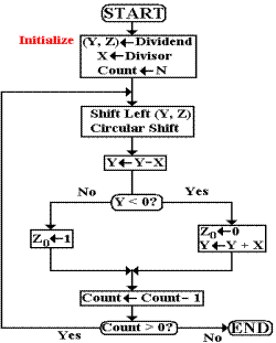
Note the
key operation, which is Y ¬ Y – X. If the
new value is not less than zero, a 1 is
placed in the least significant bit of register Z. If the new value is negative, the value X is
added back in order to restore the old value of Y. For this reason, the algorithm is called
“restoring division”.
Before
giving an example of the algorithm, we must attend to an apparent difference
between
this algorithm and the mathematics on which it is based. The key operation is standard
two’s–complement subtraction; take the two’s–complement of X and add it to
Y. This seems
to involve three registers (X, Y, and Z) as shown in the figure below.

As (Y, Z)
are being considered as a single 2N–bit register, one might ask what is so
special
about the more significant N bits. The
answer is a trick of two’s–complement arithmetic.
The basic
mathematics calls for two 2N–bit registers: the 2N–bit register pair (Y, Z) and
the
X register extended to 2N bits by padding the value with N bits to the
right. For example,
consider the 4–bit example that will be discussed later in this chapter.
X = 0111 (Decimal 7)
Y = 0010
Z = 1001 (Y, Z), as an 8–bit number, have
decimal value 41.
The algorithm defined above seems to call for the following situation.
|
0010 |
1001 |
|
0111 |
|
The precise mathematical definition calls for this situation.
|
0010 |
1001 |
|
0111 |
0000 |
The precise mathematical procedure calls
for subtracting the 2N–bit (here 8 bit) value at
bottom from the 2N–bit (here 8 bit) value in the (Y, Z) register pair. To see why the first
scheme works, we should consider the two’s–complement of the extended X
register.
For this specific example, we have the following.
The X
register proper 0111
The one’s–complement 1000
The two’s–complement 1001
The extended X register 0111 0000
The one’s–complement 1000 1111
The
two’s–complement 1001
0000
Adding the
two’s–complement of the extended X register, possibly denoted as (X, 0), has
the identical effect to adding the two’s–complement of X to Y and not changing
Z. This is
precisely what the machine algorithm calls for.
To place
this illustrative argument on slightly more solid ground, we present the sketch
of
a theoretical demonstration. Let X have
N bits, XN–1….X0, and the extended X register have
2N bits: the original X register with N 0’s appended to the right.
In taking the two’s–complement of the extended X register, we begin with the following.
![]()
The first step is to take the one’s–complement, giving the following results.
![]()
The next step is to add 1 to
this 2N–bit number. This causes all of
the N bits to the right
with value 1 to be changed to 0, and a 1 to be carried into the X0
position.
![]()
This is precisely the same as taking the two’s–complement of X and appending the zeroes.
In our
illustration of the division algorithm, we shall take a shortcut that is not
available to a
standard ALU. The first subtraction, Y ¬ Y –
X, is tentative. If the result is
negative, the
subtraction is undone by a restoring addition.
Our illustration will use the rule as follows.
If Y < X, then set Z0 = 0, else set Z0 = 1 and set Y ¬ Y –
X. Here is the procedure.
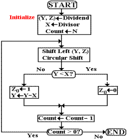
Here is the computation (0010, 1001) divided by 0111. In decimal 41 / 7 = 5, remainder 6.
Start
with (Y,Z) 0010 1001
X 0111
Shift
left (Y,Z) 0101 0010
X 0111
X is bigger. Set Z0 =
0.
Shift
left (Y,Z) 1010 0100
-X 1001 2’s-comp of 0111 is 1001
0011 0100 New value of Y
0011 0101 Set Z0 = 1.
Shift
left (Y,Z) 0110 1010
X 0111
X is bigger. Set Z0 =
0.
Shift
left (Y,Z) 1101 0100
-X 1001 2’s-comp of 0111 is 1001
0110 0100 New value of Y
0110 0101 Set Z0 = 1.
At the end,
we have Z = 0101 (the quotient is 5) and Y = 0110 (the remainder is 6).
The value in the X register has not changed.
I just display –X in the example because I
have difficulty with binary subtraction, much preferring to add the complement.
The Shifter
This section focuses on a common implementation of a shift unit, which is a circuit for achieving multiple shifts of a number of useful types. There are a several types of shifters; we shall study the simpler one that uses log2N stages to achieve shifts by N places.
We shall first discuss the logical bases for the shifting operations and then design a sequence of shifters, each more capable that the last, in order to arrive at the final design. Along the way, we note that the main problem will be the complexity of the drawings.
Types of Shifts
In general, there are two types of shifts – left shifts and right shifts. These names correspond roughly to the way in which we would illustrate these shifts by drawing diagrams. Each of the two shift types comes in three varieties: logical, circular, and arithmetic.
The basic definition of each shift type is in terms of shifting by one place. We should note that multiple shifts are easily defined; shifting by N places must be equivalent to N single shifts. For convenience in designing a barrel shifter, we normally think in terms of shifting by N = a power of two, so that a shift by 13 places is a shift by 1 place, followed by a shift by 4 places, and then a shift by 8 places, as 13 = 1 + 4 + 8.
We shall illustrate the shift types by considering them as applied to an eight-bit shift register, with contents labeled as R7 R6 R5 R4 R3 R2 R1 R0. We use 1001 0110 as an example.
Logical Shifts
Logical shifts just move bits in the indicated direction, padding out with 0’s. Shifts can be by any count, but shifts by more than the size of the register leave it all 0’s.
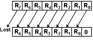 For
left shifting an N-bit register by 1 place
RJ+1 ¬ RJ for 0 £ J < (N – 1)
R0 ¬ 0, R(N
– 1) is lost
As an example of a shift of an 8-bit register
1001 0110 becomes 0010 1100
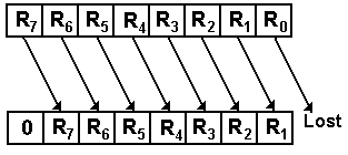
For right shifts by 1 place
RJ+1 ® RJ for 0 £ J < (N – 1)
R(N – 1) ¬ 0, R0
is lost
As an example of a 8-bit register shift
1001 0110 becomes 0100 1011
Left shift
by 2 places: 1001 0110 becomes
0101 1000
Right shift by 2 places: 1001 0110 becomes 0010 0101
Note that shifting either left or right by eight or more places produces the result 0000 0000, so that the shift count will normally be in the range 0 through 7 inclusive.
The general rule for an N-bit register is that the shift count is usually in the range from 0 to (N – 1) inclusive, a modulo-N non-negative number.
Arithmetic Shifts
Arithmetic shifts are identical to logical shifts except that the sign bits are preserved. Arithmetic shifting is normally defined only for right shifts.
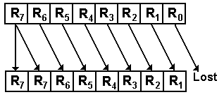
For right shifts by 1 place
RJ+1 ® RJ for 0 £ J < (N – 1)
R(N – 1) ® R(N
– 1), R0 is lost
As an example of an 8-bit register
1001 0110 becomes 1100 1011
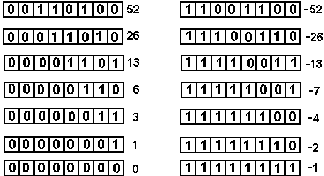
The purpose of arithmetic shifts is to cause the right shift to become equivalent to division by two on two’s-complement integers. We use 8-bit two’s-complement arithmetic to illustrate the correspondence of shifting to multiplication and division. The range of this representation is from – 128 to 127 inclusive.
Consider the number 52, represented as 0011 0100 in binary. Taking the two’s-complement of this binary pattern, we find that the representation of – 52 is 1100 1100.
We first apply successive arithmetic right shifts to both 52 and – 52.
We now apply successive logical left shifts to the same two numbers.
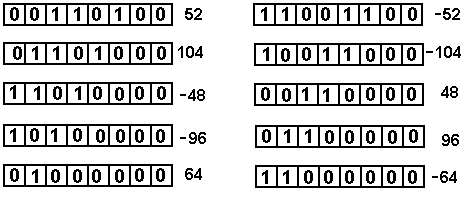
Note that this corresponds to multiplication by two whenever the sign bit stays the same.
Circular Shifts
Circular shifts are identical to logical shifts except that bits “shifted off” one end are put at the other end, thus making the shift appear as a circle.
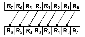
For left shifts by 1 place
RJ+1 ¬ RJ for 0 £ J < (N – 1) R0 ¬ R(N – 1), nothing
is lost
As an example for an 8-bit shift
1001 0110 becomes 0010 1101
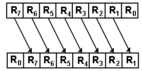 For
right shifts by 1 place
RJ+1 ® RJ for 0 £ J < (N – 1)
R(N – 1) ¬ R0
As an example of an 8-bit shift
1001 0110 becomes 0100 1011
Circular shifts are quite often used when writing code for
device drivers. These drivers assign
bits in a word as logical flags. Suppose
that bits 3 and 2 of an 8-bit register contain a device select. We would right shift by two to get the bits
into position and do a logical
Example: Let R = 0010
0101
Right shift by 2 0100 1001
AND 0000 0011 0000 0001 The selected device is 01.
Logical Left Shift
We begin our study of barrel shifters by presenting a very
simple logical left shift circuit. As
this author had to draw the circuit, it is presented as a four-bit shifter
taking input X3X2X1X0 and
outputting Y3Y2Y1Y0. This shifter is controlled by a signal named
“SHIFT”.
If SHIFT = 0, the circuit is a
copy.
If SHIFT = 1, the circuit
performs a left shift by one position.
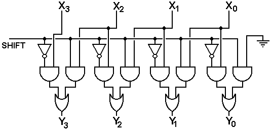
The basic element in this circuit is the shifter comprising two AND gates and an OR gate. The SHIFT control signal here is designated by S. There are two inputs
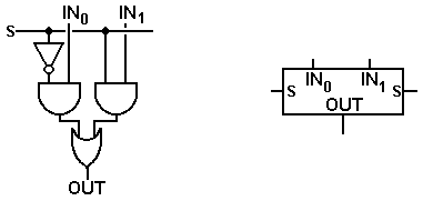
When S = 0, the input labeled IN0 is passed to
the output; when S = 1, the input labeled IN1 is passed to the
output. In the above circuit, we have
the following connections:
For 1 £ N £ 3 IN0 is connected to XN
IN1 is connected to XN–1
For N = 0 IN0 is connected
to X0
IN1
is connected to 0.
In order to simplify our drawings, we use the symbol at the right to represent this simple shift/pass-through circuit. Note that the input S is output by the element as input.
We now present the simple left shifter diagram using our new circuit element.

The reason for the unusual alignment of the input will become obvious in the next discussion. Note that each element passes the SHIFT control signal to the next one. This is a convention used in the diagram to avoid drawing too many crossing lines.
Logical Left Shifter for Multiple Shifts
We now present a shifter that will shift left by 0, 1, 2, or 3 places. The amount of the shift is controlled by the binary number S1S0.
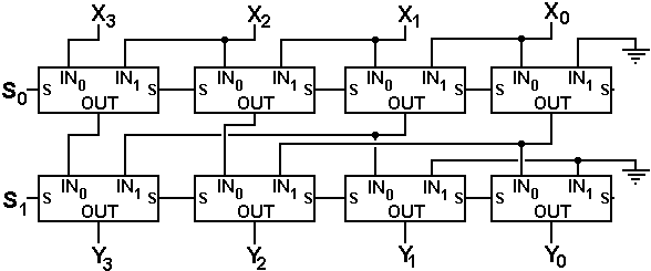
The shift is
implemented in two stages, the first stage shifting by either 0 or 1, and the
second stage shifting by either 0 or 2.
This is basically a barrel shifter.
The rules are
Signals Action Top Unit Bottom Unit
S1 = 0 S0
= 0 No shift No shift No shift
S1 = 0 S0 = 1 Left shift one place Shift
by 1 No shift
S1 = 1 S0 = 0 Left shift two places No
shift Shift by 2
S1 = 1 S0 = 1 Left shift three places Shift
by 1 Shift by 2
Allowing Circular Shifts
We now make a modification to allow selection between circular and logical shifts.
The control signal is C. If C = 0, the shift is logical. If C = 1 the shift is circular.
One should note that even this simple shifter is associated with a circuit diagram that is increasingly hard to read.
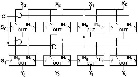
The Two-Level 4-Bit Barrel Shifter
Another Implementation of A Left Shifter
We now present an implementation of a four-bit logical left shifter with 4-to-1 multiplexers.
Each output has a selection of four inputs, depending on the shift count. As above, C is the circulate control, with C = 0 for logical shifts and C = 1 for circular shifts. The shift count is specified by the binary number S1S0, which is passed on by each multiplexer to the next one.
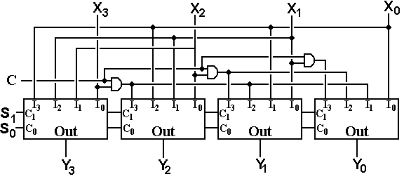
The Multiplexer-Based 4-Bit Barrel Shifter
Another Look at the 4-bit
Shifter
Our presentation of the barrel shifter will be based on the design that uses multiple levels of two-input shift units. The representation of this design, as shown above, works well for 4-bit shifters, but will become complex for a 32-bit shifter. For that reason, we show two simpler representations of the two-level four-bit barrel shifter.
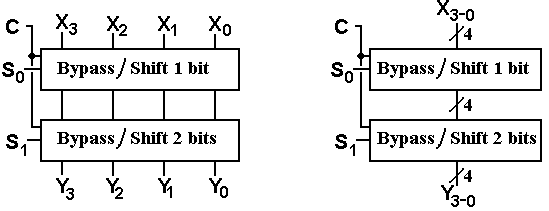
Simpler Representations of the Two-Level
Four-Bit Barrel Shifter
The design on the left shows the barrel shifter with each level of four shift units grouped into a single block labeled by its functionality. The figure on the right is drawn in the simplest style possible. This is the representation that we shall use.
A 32-bit Left Shifter
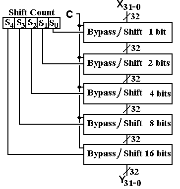
The figure on the right shows the general 32-bit left shifter as we shall draw such figures in order to minimize complexity. Note that it comprises five shifting levels, one each for shifts by 1, 2, 4, 8, and 16 bits. Each level is controlled by one bit of the five bit shift-count register. In a more general CPU design, this shift count register will be a part of the Instruction Register (IR). Note the control signal C, which continues to stand for Circular: C = 0 for a logical shift and C = 1 for a circular shift.
Logical Right Shift
As before, we begin with a basic AND/OR/NOT circuit implementing the logical right shift. Note that this is almost a mirror-image of the logical left shifter.
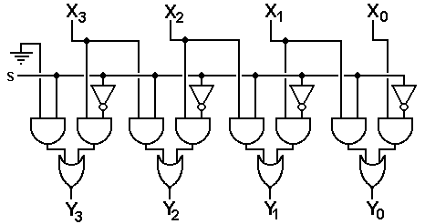
Right Shift: Logical,
Arithmetic, and Circular
We now add two control
signals, A for Arithmetic Shift and C for Circular Shift. Neither of these will have effect if S = 0,
calling for no shift. When S = 1, the
following holds
A = d C = 1 Circular right
shift. This is an arbitrary decision,
but the signals
A and
C should not be asserted simultaneously.
A = 1 C = 0 Arithmetic
right shift
A = 0 C = 0 Logical right
shift
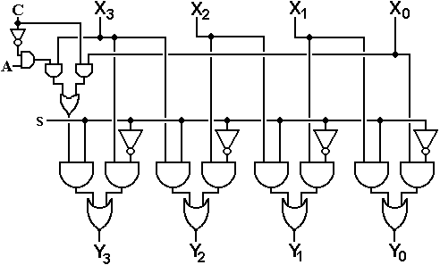
In order to understand the above circuit, consider the input to the left AND gate corresponding to the Y3 output. This gate is active when S = 1, indicating a shift.
The operative part of the circuit, providing input when S = 1 is shown below.
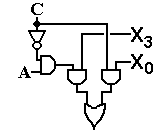
From the above diagram we derive the truth table shown below. The student should understand that the action for the condition A = 1 and C = 1 was decided by which decision would yield the neater drawing, not by any deep consideration of architectural details.
|
A |
C |
Input |
|
0 |
0 |
0 |
|
0 |
1 |
X0 |
|
1 |
0 |
X3 |
|
1 |
1 |
X0 |
The above circuit, while logically correct, “misses the forest for the trees” in that it overlooks an obvious simplification in the circuitry. What we have in the first try at the circuit for Y3 input is an OR gate feeding another OR gate. This can be simplified.
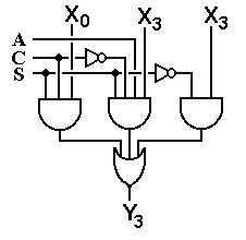
We now trace the output of the revised and simplified circuit. When S = 0, there is no shift.
If S = 0 then
Y3 = X3 (no shift), as expected.
If S = 1 and C = 1 then Y3 = X0
– for a circular shift
If S = 1, C = 0, and A = 1 then Y3 = X3
(copy the sign bit) for an arithmetic shift.
If S = 1, C = 0, and A = 0 then Y3 = 0, for a
logical right shift.
Again, the precedence of C = 1 over A = 1 is an arbitrary design decision
Here is the shift-by-one level slightly redrawn to facilitate readability.
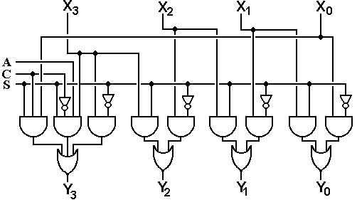
A barrel shifter for right shifts by two is a bit more complex.
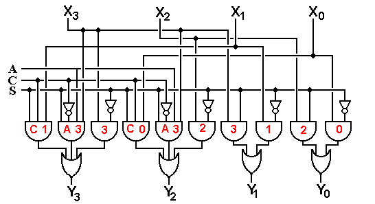
In the diagram above, each AND gate has been labeled with the input to which it corresponds. Again, all we really need to worry about is the complexity.
Here is the two-level barrel shifter capable of shifting right by 0, 1, 2, or 3 places.
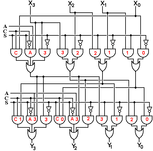
Shown below is the two-level simplification of the above circuit.
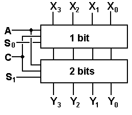
Here is the version of the shifter that we shall use in future work. There are a number of control inputs to this circuit that determine the shifting of X31-0 to produce Y31-0.
The shift count is a five-bit binary number, ranging in value from 0 through 31 inclusive.
There are three control
signals:
![]() the shift
direction: 0 for right shift and 1 for left shift
the shift
direction: 0 for right shift and 1 for left shift
A the arithmetic shift flag, this applies
only to right shifts.
If A = 1, we have
an arithmetic shift (if ![]() = 0)
= 0)
C the circular shift flag. If C = 1 we have a circular shift.
Recall that we have arbitrarily decided to do a circular shift if both A = 1 and C = 1. The only requirement for this circuit is that when both shift signals are asserted, only one is done.
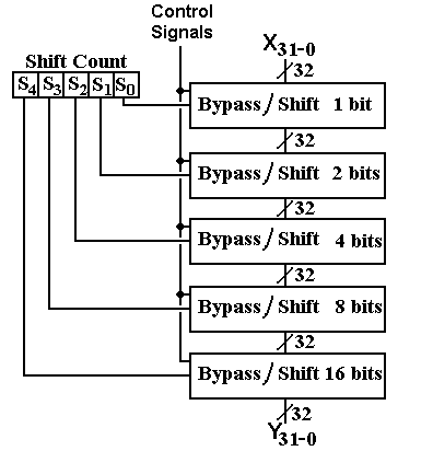
Commercial
Chips
This
section of the chapter will discuss some commercial MSI chips that once were
used to
implement ALUs and MDUs. While these
units are no longer in use, they seem to form the
logical basis for the modern ALU/MDU designs, and so will be studied. The chips to be
studied are the SN74181 ALU and the CDP1855 MDU.
In order to
emphasize the point above, we examine two pictures: one a labeled picture of a
Pentium CPU (taken in 1993), and the other a picture of a PDP–11 CPU (vintage
1980’s).
Here is the labeled picture of
the Pentium CPU. The ALU and MDU are
contained in the
block labeled “Superscalar Integer Execution Units”.
Here is a picture of the PDP–11 CPU, which contains several SN74121 ALU chips.
What one
should notice is that the entire Pentium CPU chip would easily fit within one
of
the gold squares to the upper left of the PDP–11 CPU board. The Pentium CPU is much
smaller, very much faster, and much more powerful. The MSI chips we shall discuss are
physically too big for modern hardware; their only relevance is logical design.
The SN74181 ALU Chip
This chip
was discussed in Chapter 1 (pages 50–52) as an example of a MSI chip. That
chapter includes a picture of the chip, dimensional drawings, and a circuit
diagram. As this
chip has influenced more modern designs, we shall discuss its functionality.
Here is the
function table for the SN74181, assuming active–high inputs and outputs.
Note that the output is determined by the logic mode bit, M, and the selectors
S3S2S1S0.
|
Mode Select Inputs |
Active High Inputs and Outputs |
||||
|
S3 |
S2 |
S1 |
S0 |
Logic Mode (M = 1) |
Arithmetic (M = 0, Cin = 1) |
|
0 |
0 |
0 |
0 |
A’ |
A |
|
0 |
0 |
0 |
1 |
(A + B)’ |
A + B |
|
0 |
0 |
1 |
0 |
A’·B |
A + B’ |
|
0 |
0 |
1 |
1 |
Logical 0 |
Minus 1 |
|
0 |
1 |
0 |
0 |
(A·B)’ |
A plus A·B’ |
|
0 |
1 |
0 |
1 |
B’ |
(A + B) plus A·B’ |
|
0 |
1 |
1 |
0 |
A Å B |
A minus B minus 1 |
|
0 |
1 |
1 |
1 |
A·B’ |
A·B’ minus 1 |
|
1 |
0 |
0 |
0 |
A’ + B |
A plus A·B |
|
1 |
0 |
0 |
1 |
(A Å B)’ |
A plus B |
|
1 |
0 |
1 |
0 |
B |
(A + B’) plus A·B |
|
1 |
0 |
1 |
1 |
A·B |
A·B minus 1 |
|
1 |
1 |
0 |
0 |
Logical 1 |
A plus A (2A) |
|
1 |
1 |
0 |
1 |
A + B’ |
(A + B) plus A |
|
1 |
1 |
1 |
0 |
A + B |
(A + B’) plus A |
|
1 |
1 |
1 |
1 |
A |
A minus 1 |
The vast array of functions available is
probably a result of the design chosen.
The goal
seems to have been to create a simple design that would result in the desired
functionality.
The “extra functions” were probably the result of the simplicity of the design.
The control
unit of a design based on the SN74181 would probably issue control signals for
only a small subset of the possible functions.
The design for the Boz–7 computer and later
designs will use an ALU designed by the instructor. While the Boz–7 ALU is probably not
as good as the SN74181, it is considerably easier to explain.
The
CDP1855 MDU Chip
The CDP1855 is a CMOS 8–bit multiply/divide unit. These chips can be grouped in twos or fours to provide either 16–bit or 32–bit functionality.
Each CDP1855
has number of 8–bit registers, four of which concern us directly. These
are the Control Register, and the three data registers: X, Y, and Z.
For
multiplication, the 8–bit multiplicand and multiplier are placed in registers X
and Z,
with the 16–bit product found in the 16–bit register pair (Y, Z).
For
division, the 16–bit dividend is placed in the 16–bit register pair (Y, Z) and
the 8–bit
divisor is placed in the 8–bit register X.
After division, the 8–bit quotient is found in the
8–bit register Z, and the 8–bit remainder is found in 8–bit register Y.
The interesting parts of the Control Register are bits 5 and 4, and bits 1 and 0.
Bits 1 and 0 select the operation to be performed.
|
Bit 1 |
Bit 0 |
Operation |
|
0 |
0 |
No operation |
|
0 |
1 |
Multiply |
|
1 |
0 |
Divide |
|
1 |
1 |
Illegal |
A realistic use of the CDP1855 would
specify that input 11 here would be mapped to
either 01 (multiply dominates) or 10 (divide dominates).
Bits 5 and 4 determine the
number of CDP1855 chips being used in this particular MDU
implementation. This setting determines
the internal clock rates for each CDP1855.
|
Bit 5 |
Bit 4 |
Number
of CDP1855 |
|
1 |
1 |
Four |
|
1 |
0 |
Three |
|
0 |
1 |
Two |
|
0 |
0 |
One |
One important feature for using the MDU is to note the relative lengths of the numbers involved. Consider a “32–bit unit”. Here are the actual lengths.
For multiplication the multiplicand and multiplier are each 32 bits in length,
and
the
product is 64 bits in length.
For division the dividend is 64 bits in length, and
each
of the dividend, quotient, and remainder is 32 bits in length.
In a load/store RISC design, such as used by this author’s design, all arithmetic is done between registers. This author’s design calls for integers stored in two’s–complement form in 32–bit registers.
The solution for the 64–bit product and dividend is one that this author has borrowed from the assembly language for IBM mainframe computers, such as the z/10. It may be much more common than that. 64–bit integers will be stored in (even, odd) register pairs. For example, a 64–bit dividend stored in the register pair denoted by 6 would have the high order 32 bits stored in register 6 and the low order 32 bits stored in register 7.
The rationale behind the use of the
(even, odd) register pair design is that it facilitates the design of the
control unit. It appears obvious that
the register pair should be of the form
(R, R + 1), such as (4, 5). If the first
register is an even number, one may just set the last bit to 1 and effectively
add 1 to the number.
Register 6 110
Register 7 111.
Solved Problems
We now present some solved problems.
PROBLEM
1. Given a function represented by the truth table
|
X |
Y |
Z |
F(X, Y, Z) |
|
0 |
0 |
0 |
0 |
|
0 |
0 |
1 |
1 |
|
0 |
1 |
0 |
1 |
|
0 |
1 |
1 |
0 |
|
1 |
0 |
0 |
1 |
|
1 |
0 |
1 |
1 |
|
1 |
1 |
0 |
0 |
|
1 |
1 |
1 |
1 |
Implement this function using an 8-to-1 multiplexer and no other logic gates.
ANSWER: We use an eight-to-one
multiplexer with three control lines C2, C1, and C0. Because we list X, Y, Z in that order in the
function, we set C2 = X, C1 = Y, and C0 =
Z. Note that all inputs must be
specified – either connected to logic 1 or logic 0.
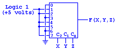
The next two questions concern the function represented by F(A, B, C) = S(0, 2, 3, 5, 6, 7).
3. Implement this function using an 8-to-1 multiplexer.
Answer:
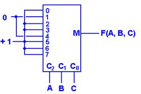
4. Implement this function using a 3-to-8 active–high decoder and a single NOR gate.
ANSWER: This function can be written as F(A, B, C) = P(1, 4), that is it has the
value 0 only for the rows 0 and 4 in the truth table: A = 0, B = 0, C = 1, and
A = 1, B = 0, C = 0.
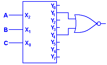
The next two questions focus on a Boolean function F(W, X, Y, Z) = S(0, 3, 5, 8, A, B, C)
5 Use an active-high 4-to-16 decoder and OR gates to implement this function.
6 Use a 16-to-1 multiplexer to implement this function.
ANSWER:
Here are the two circuits. A 7-input OR
gate would be acceptable.
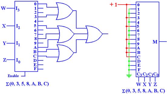
7 An active-low
decoder is one in which the selected output goes to zero and
the other outputs remain at 1. Here is the description of an enabled-low, active-low
2-to-4 decoder. Implement this decoder using only AND, OR,
and NOT gates.
Enable = 0 X1 = 0 X0
= 0 Y0 = 0 Y1 = 1 Y2 = 1 Y3 = 1
Enable = 0 X1 = 0 X0
= 1 Y0 = 1 Y1 = 0 Y2 = 1 Y3 = 1
Enable = 0 X1 = 1 X0
= 0 Y0 = 1 Y1 = 1 Y2 = 0 Y3 = 1
Enable = 0 X1 = 1 X0
= 1 Y0 = 1 Y1 = 1 Y2 = 1 Y3 = 0
Enable = 1 X1 = d X0
= d Y0 = 1 Y1 = 1 Y2 = 1 Y3 = 1
The circuit must have three inputs (Enable, X1, and X0) and four outputs.
ANSWER: The easiest
way to do this is first ignore the Enable and draw the truth table. Basically, we have four truth tables. Lets examine them as a group and then
individually.
|
X1 |
X0 |
Y0 |
Y1 |
Y2 |
Y3 |
|
0 |
0 |
0 |
1 |
1 |
1 |
|
0 |
1 |
1 |
0 |
1 |
1 |
|
1 |
0 |
1 |
1 |
0 |
1 |
|
1 |
1 |
1 |
1 |
1 |
0 |
Examining the
four functions represented in the truth table, we see that each has exactly one
zero and three one’s in its column. This
should immediately suggest POS (Product of Sums) formulations for each
function. Let’s look at the first
function: Y0.
|
X1 |
X0 |
Y0 |
Sum Term |
|
0 |
0 |
0 |
X1 + X0 |
|
0 |
1 |
1 |
|
|
1 |
0 |
1 |
|
|
1 |
1 |
1 |
|
As an aside,
note that the truth table for Y0 is exactly the truth table for the expression
(X1 + X0). This is the reason for making
the association of the sum term to the row.
Here are the
other three truth tables.
|
X1 |
X0 |
Y1 |
Sum Term |
|
0 |
0 |
1 |
|
|
0 |
1 |
0 |
X1 + X0’ |
|
1 |
0 |
1 |
|
|
1 |
1 |
1 |
|
|
X1 |
X0 |
Y2 |
Sum Term |
|
0 |
0 |
1 |
|
|
0 |
1 |
1 |
|
|
1 |
0 |
0 |
X1’ + X0 |
|
1 |
1 |
1 |
|
|
X1 |
X0 |
Y3 |
Sum Term |
|
0 |
0 |
1 |
|
|
0 |
1 |
1 |
|
|
1 |
0 |
1 |
|
|
1 |
1 |
0 |
X1’ + X0’ |
Without
the enable input, we have the four equations.
Y0 = X1 + X0
Y1 = X1 + X0’
Y2 = X1’ + X0
Y3 = X1’ + X0’
Now,
all we need is a way for the Enable signal to force all four of these to 1 when
E = 1. This is easily done with an OR
gate.
Y0 = E + X1 + X0
Y1 = E + X1 + X0’
Y2 = E + X1’ + X0
Y3 = E + X1’ + X0’
We now show a
circuit that implements these four Boolean functions.
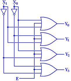
We
now investigate whether or not there is another implementation of this
circuit. To do this, we look at using
either AND or OR gates to implement this circuit, and postulate a new signal,
called A, that is related to the
Enable signal. We look at the two basic
possibilities.
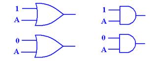
The
rules of the game are simple. Either A = 0 means enabled or A = 1 means enabled. Either 1 or 0 means “select me”. The requirement on the two circuits is quite
simple also: for one value of A,
both outputs are the same, and for another value of A, one output is 1 and the other is 0. Once we have this, we can determine what A must be.
For the OR gates, a value of A = 1 makes all outputs equal
1. Thus the “select me” value must be 0
and A = 0 must be the enable signal. For
the AND gates, a value of A = 0 makes all outputs equal 0. Thus the “select me” value must be 1 and A =
1 must be the enable.
The statement of the problem requires that the “select me”
signal be 0, so the AND gates must be changed to NAND gates or followed by a
NOT gate. The new circuits are:
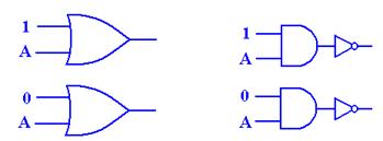
For
the OR gate circuits on the left,
A = 0 => the “selected” output is 0 and the other is 1
A = 1 => all outputs are 1.
For
the NAND (AND followed by NOT) gate circuits on the right.
A = 0 => all outputs are 1
A = 1 => the “selected” output is 0 and the other is 1.
Use
of the OR gate strategy, as on the left, gives rise to the circuit shown
above. Use of the NAND gate strategy, as
on the right, gives rise to the other valid implementation.
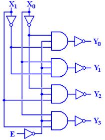
8 Consider a computer in which all integers are stored as 8 bits.
a) What
is the range of integer values that can be stored in two’s–complement form;
i.e. the most negative integer
and the most positive integer.
b) What is the range of integer values that can be stored for unsigned arithmetic.
c) Perform
the following sums assuming 8–bit binary arithmetic.
Indicate the answer as
“Overflow” if the sum cannot be represented.
i) 120 + 130 (assuming
unsigned arithmetic)
ii) 120 + 130 (assuming
saturation arithmetic)
iii) 140 + 150 (assuming
unsigned arithmetic)
iv) 140 + 150 (assuming
saturation arithmetic)
NOTE: You can answer this
without doing any binary arithmetic.
a) The range for signed 8-bit integers is given as follows:
Two’s-complement – 128 through 127
inclusive.
b) The range for signed 8-bit integers is given as follows:
Unsigned arithmetic 0 through 255 inclusive.
c) 120 + 130 = 250
120 + 130 = 250
140 + 150 = OVERFLOW
140 + 150 = 255 (Saturation)
PROBLEMS FOR SOLUTION
1. Design and implement a 2-to-4 decoder using only AND, OR, and NOT gates.
2. Design and implement a 4-to-1 multiplexer using only AND, OR, and NOT gates.
The next few problems are based on the following truth table.
|
A |
B |
C |
F(A, B, C) |
|
0 |
0 |
0 |
0 |
|
0 |
0 |
1 |
1 |
|
0 |
1 |
0 |
1 |
|
0 |
1 |
1 |
0 |
|
1 |
0 |
0 |
1 |
|
1 |
0 |
1 |
1 |
|
1 |
1 |
0 |
0 |
|
1 |
1 |
1 |
1 |
3. Use a 3-to-8 decoder and a single 5-input OR gate to realize this
function.
In other words, use these gates to
design a circuit for this function.
4. Use a 3-to-8 decoder and a single 3-input NOR gate to realize this function.
5. Use an 8-to-1 multiplexer to realize this function.
6. An enabled-low active-high decoder is one for which all outputs
are inactive (equal
logic 0) when Enable = 1 and for
which only the selected output is active (equal
logic 1) when Enable = 0. Use a 1-to-4 demultiplexer to realize this
circuit.