The usage of the term “RAM” for the type of random access memory that might well be called “RWM” has a long history and will be continued in this course. The basic reason is probably that the terms “RAM” and “ROM” can easily be pronounced; try pronouncing “RWM”. Keep in mind that both RAM and ROM are random access memory.
Of course, there is no such thing as a pure Read-Only memory; at some time it must be possible to put data in the memory by writing to it, otherwise there will be no data in the memory to be read. The term “Read-Only” usually refers to the method for access by the CPU. All variants of ROM share the feature that their contents cannot be changed by normal CPU write operations. All variants of RAM (really Read-Write Memory) share the feature that their contents can be changed by normal CPU write operations. Some forms of ROM have their contents set at time of manufacture, other types called PROM (Programmable ROM), can have contents changed by special devices called PROM Programmers.
Registers associated with the memory system
All memory types, both RAM and ROM can be characterized by
two registers and a number of control signals.
Consider a memory of 2N words, each having M bits. Then
the MAR (Memory Address
Register) is an N-bit register used to specify the
memory address
the MBR (Memory Buffer
Register) is an M-bit register used to hold data to
be written to the
memory or just read from the memory.
This register is
also called the
MDR (Memory Data Register).
We specify the control signals to the memory unit by
recalling what we need the unit to do.
First consider RAM (Read Write Memory).
From the viewpoint of the CPU there are three tasks for the memory
CPU reads data from the
memory. Memory contents are not changed.
CPU writes data to the memory. Memory contents are updated.
CPU does not access the
memory. Memory contents are not changed.
We need two control signals to specify the three options for a RAM unit. One standard set is
Select – the memory unit is selected.
![]() – if 0 the CPU writes
to memory, if 1 the CPU reads from memory.
– if 0 the CPU writes
to memory, if 1 the CPU reads from memory.
We can use a truth table to specify the actions for a RAM. Note that when Select = 0,
|
Select |
|
Action |
|
0 |
0 |
Memory contents are not changed. |
|
0 |
1 |
Memory contents are not changed. |
|
1 |
0 |
CPU writes data to the memory. |
|
1 |
1 |
CPU reads data from the memory. |
nothing is happening to the memory. It is not being accessed by the CPU and the contents do not change. When Select = 1, the memory is active and something happens.
Consider now a ROM (Read Only Memory). Form the viewpoint of the CPU there are only
two tasks for the memory
CPU reads data from the
memory.
CPU does not access the
memory.
We need only one control signal to specify these two
options. The natural choice is the
Select control signal as the ![]() signal does not make
sense if the memory cannot be written by the CPU. The truth table for the ROM should be obvious
signal does not make
sense if the memory cannot be written by the CPU. The truth table for the ROM should be obvious
|
Select |
Action |
|
0 |
CPU is not accessing the memory. |
|
1 |
CPU reads data from the memory. |
The Idea of Address Space
We now must distinguish between the idea of address space and physical memory. The address space defines the range of addresses (indices into the memory array) that can be generated. The size of the physical memory is usually somewhat smaller, this may be by design (see the discussion of memory-mapped I/O below) or just by accident.
An N–bit address will specify 2N different addresses. In this sense, the address can be viewed as an N–bit unsigned integer; the range of which is 0 to 2N – 1 inclusive. We can ask another question: given M addressable items, how many address bits are required. The answer is given by the equation 2(N - 1) < M £ 2N, which is best solved by guessing N.
The memory address is specified by a binary number placed in the Memory Address Register (MAR). The number of bits in the MAR determines the range of addresses that can be generated. N address lines can be used to specify 2N distinct addresses, numbered 0 through 2N – 1. This is called the address space of the computer.
For example, we show three MAR sizes.
Computer |
MAR bits |
|
|
PDP-11/20 |
16 |
0 to 65 535 |
|
Intel 8086 |
20 |
0 to 1 048 575 |
|
Intel Pentium |
32 |
0 to 4 294 967 295 |
The PDP-11/20 was an elegant small machine made by the now defunct Digital Equipment Corporation. As soon as it was built, people realized that its address range was too small.
In general, the address space is much larger than the physical memory available. For example, my personal computer has an address space of 232 (as do all Pentiums), but only 384MB = 228 + 227 bytes. Until recently the 32–bit address space would have been much larger than any possible amount of physical memory. At present one can go to a number of companies and order a computer with a fully populated address space; i.e., 4 GB of physical memory. Most high-end personal computers are shipped with 1GB of memory.
In a design with memory-mapped I/O part of the address space is dedicated to addressing I/O registers and not physical memory. For example, in the original PDP–11/20, the top 4096 (212) of the address space was dedicated to I/O registers, leading to the memory map.
Addresses 0
– 61439 Available for physical memory
Addresses 61440 – 61535 Available for I/O registers (61440 =
61536 – 4096)
Word Addresses in a
Byte-Addressable Machine
Most computers today have memories that are byte-addressable; thus each byte in the memory has a unique address that can be used to address it. Under this addressing scheme, a word corresponds to a number of addresses.
A 16–bit word at address Z contains bytes at addresses Z and Z + 1.
A 32–bit word at address Z contains bytes at addresses Z, Z + 1, Z + 2, and Z + 3.
In many computers with byte addressing, there are constraints on word addresses.
A 16–bit word must have an even address
A 32–bit word must have an address
that is a multiple of 4.
Even in computers that do not enforce this requirement, it is a good idea to observe these word boundaries. Most compilers will do so automatically.
Suppose a byte-addressable
computer with a 32-bit address space.
The highest byte address is 232 – 1. From this fact and the address allocation to
multi-byte words, we conclude
the highest address for a 16-bit
word is (232 – 2), and
the highest address for a 32-bit word is (232 – 4), because the 32-bit word addressed at (232 – 4) comprises bytes at addresses (232 – 4), (232 – 3), (232 – 2), and (232 – 1).
Byte Addressing vs. Word Addressing
We have noted above that N address lines can be used to specify 2N distinct addresses, numbered 0 through 2N – 1. We now ask about the size of the addressable items. We have seen that most modern computers are byte-addressable; the size of the addressable item is therefore 8 bits or one byte. There are other possibilities. We now consider the advantages and drawbacks of having larger entities being addressable.
As a simple example, consider a computer with a 16–bit address space. The machine would have 65,536 (64K = 216) addressable entities. The maximum memory size would depend on the size of the addressable entity.
Byte Addressable 64 KB
16-bit Word Addressable 128 KB
32-bit Word Addressable 256 KB
For a given address space, the maximum memory size is greater for the larger addressable entities. This may be an advantage for certain applications, although this advantage is reduced by the very large address spaces we now have: 32–bits now and 64–bits soon.
The advantages of byte-addressability are clear when we consider applications that process data one byte at a time. Access of a single byte in a byte-addressable system requires only the issuing of a single address. In a 16–bit word addressable system, it is necessary first to compute the address of the word containing the byte, fetch that word, and then extract the byte from the two-byte word. Although the processes for byte extraction are well understood, they are less efficient than directly accessing the byte. For this reason, many modern machines are byte addressable.
Big-Endian and Little-Endian
The reference here is to a story in Gulliver’s Travels written by Jonathan Swift in which two groups of men went to war over which end of a boiled egg should be broken – the big end or the little end. The student should be aware that Swift did not write pretty stories for children but focused on biting satire; his work A Modest Proposal is an excellent example.
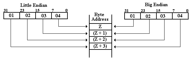
Consider the 32–bit number
represented by the eight–digit hexadecimal number 0x01020304, stored at
location Z in memory. In all
byte-addressable memory locations, this number will be stored in the four
consecutive addresses Z, (Z + 1), (Z + 2), and (Z + 3). The difference between big-endian and
little-endian addresses is where each of the four bytes is stored. In our example 0x01 represents bits 31 – 24, 0x02 represents bits 23 – 16,
0x03 represents
bits 15 – 8, and 0x04 represents
bits 7 – 0 of the word.
As a 32-bit signed integer, the number 0x01020304 can be represented in decimal notation as
1·166 + 0·165 + 2·164 + 0·163 + 3·162 + 0·161 + 4·160 = 16,777,216 + 131,072 + 768 + 4 = 16,909,060. For those who like to think in bytes, this is (01)·166 + (02)·164 + (03)·162 + 04, arriving at the same result. Note that the number can be viewed as having a “big end” and a “little end”, as in the following figure.

The “big end” contains the most significant digits of the number and the “little end” contains the least significant digits of the number. We now consider how these bytes are stored in a byte-addressable memory. Recall that each byte, comprising two hexadecimal digits, has a unique address in a byte-addressable memory, and that a 32-bit (four-byte) entry at address Z occupies the bytes at addresses Z, (Z + 1), (Z + 2), and (Z + 3). The hexadecimal values stored in these four byte addresses are shown below.
Address Big-Endian Little-Endian
Z 01 04
Z + 1 02 03
Z + 2 03 02
Z + 3 04 01
Just to be complete, consider the 16–bit number represented by the four hex digits 0A0B. Suppose that the 16-bit word is at location W; i.e., its bytes are at locations W and (W + 1). The most significant byte is 0x0A and the least significant byte is 0x0B. The values in the two addresses are shown below.
Address Big-Endian Little-Endian
W 0A 0B
W + 1 0B 0A
The figure below shows a graphical way to view these two options for ordering the bytes copied from a register into memory. We suppose a 32-bit register with bits numbered from 31 through 0. Which end is placed first in the memory – at address Z? For big-endian, the “big end” or most significant byte is first written. For little-endian, the “little end” or least significant byte is written first.
There seems to be no advantage of one system over the other. Big–endian seems more natural to most people and facilitates reading hex dumps (listings of a sequence of memory locations), although a good debugger will remove that burden from all but the unlucky.
Big-endian computers include the IBM 360 series, Motorola 68xxx, and SPARC by Sun.
Little-endian computers include the Intel Pentium and related computers.
The big-endian vs. little-endian debate is one that does not concern most of us directly. Let the computer handle its bytes in any order desired as long as it produces good results. The only direct impact on most of us will come when trying to port data from one computer to a computer of another type. Transfer over computer networks is facilitated by the fact that the network interfaces for computers will translate to and from the network standard, which is big-endian. The major difficulty will come when trying to read different file types.
The big-endian vs. little-endian debate shows in file structures when computer data are “serialized” – that is written out a byte at a time. This causes different byte orders for the same data in the same way as the ordering stored in memory. The orientation of the file structure often depends on the machine upon which the software was first developed.
The following is a partial list
of file types taken from a textbook once used by this author.
Little-endian Windows BMP, MS Paintbrush, MS RTF, GIF
Big-endian Adobe photoshop, JPEG, MacPaint
Some applications support both orientations, with a flag in the header record indicating which is the ordering used in writing the file.
Any student who is interested in the literary antecedents of the terms “big-endian” and “little-endian” may find a quotation at the end of this chapter.
The Memory
Hierarchy
As often is the case, we utilize a number of logical models of our memory system, depending on the point we want to make. The simplest view of memory is that of a monolithic linear memory; specifically a memory fabricated as a single unit (monolithic) that is organized as a singly dimensioned array (linear). This is satisfactory as a logical model, but it ignores very many issues of considerable importance.
Consider a memory in which an M–bit word is the smallest
addressable unit. For simplicity, we
assume that the memory contains N = 2K words and that the address
space is also N = 2K. The
memory can be viewed as a one-dimensional array, declared something like
Memory : Array [0 .. (N – 1)]
of M–bit word.
The monolithic view of the memory is shown in the following figure.
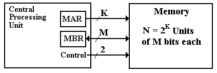
Figure: Monolithic View of Computer Memory
In this monolithic view, the CPU provides K address bits to access N = 2K memory entries, each of which has M bits, and at least two control signals to manage memory.
The linear view of memory is a way to think logically about the organization of the memory. This view has the advantage of being rather simple, but has the disadvantage of describing accurately only technologies that have long been obsolete. However, it is a consistent model that is worth mention. The following diagram illustrates the linear model.
There are two problems with the above model, a minor
nuisance and a “show–stopper”.
The minor problem is the speed of the memory; its access time will be exactly
that of plain variety DRAM (dynamic random access memory), which is
about 50 nanoseconds. We must have
better performance than that, so we go to other memory organizations.
The “show–stopper” problem is the design of the memory
decoder. Consider two examples for
common memory sizes: 1MB (220 bytes) and 4GB (232 bytes)
in a byte–oriented memory.
A 1MB memory would use a
20–to–1,048,576 decoder, as 220 = 1,048,576.
A 4GB memory would use a
32–to–4,294,967,296 decoder, as 232 = 4,294,967,296.
Neither of these decoders can be manufactured at acceptable cost using current technology. One should note that since other designs offer additional benefits, there is no motivation to undertake such a design task.
We now examine two design choices that produce easy-to-manufacture solutions that offer acceptable performance at reasonable price. The first is the memory hierarchy, using various levels of cache memory, offering faster access to main memory. Before discussing the ideas behind cache memory, we must first speak of two technologies for fabricating memory.
SRAM (Static RAM)
and DRAM (Dynamic RAM)
We now discuss technologies used to store binary information. The first topic is to make a list of requirements for devices used to implement binary memory.
1) Two well defined and
distinct states.
2) The
device must be able to switch states reliably.
3) The
probability of a spontaneous state transition must be extremely low.
4) State
switching must be as fast as possible.
5) The
device must be small and cheap so that large capacity memories are practical.
There are a number of memory technologies that were developed in the last half of the twentieth century. Most of these are now obsolete. There are three that are worth mention:
1) Core Memory (now obsolete, but new
designs may be introduced soon)
2) Static RAM
3) Dynamic RAM
Core Memory
This was a major advance when it was introduced in 1952, first used on the MIT Whirlwind. The basic memory element is a torus (tiny doughnut) of magnetic material. This torus can contain a magnetic field in one of two directions. These two distinct directions allow for a two-state device, as required to store a binary number.
One aspect of magnetic core memory remains with us – the frequent use of the term “core memory” as a synonym for the computer’s main memory.
In discussing the
next two technologies, we must make two definitions. These are memory access time and memory cycle
time. The measure of real interest is
the access time. The unit for measuring
memory times is the nanosecond, equal to one billionth of a second.
Memory access time is the time required for the memory to access the data; specifically, it is the time between the instant that the memory address is stable in the MAR and the data are available in the MBR.
Memory cycle time is the minimum time between two independent memory accesses. It should be clear that the cycle time is at least as great as the access time, because the memory cannot process an independent access while it is in the process of placing data in the MBR.
Static RAM
Static RAM (SRAM) is a memory technology based on flip-flops. SRAM has an access time of 2 – 10 nanoseconds. From a logical view, all of main memory can be viewed as fabricated from SRAM, although such a memory would be unrealistically expensive.
Dynamic RAM
Dynamic RAM (DRAM) is a memory technology based on capacitors – circuit elements that store electronic charge. Dynamic RAM is cheaper than static RAM and can be packed more densely on a computer chip, thus allowing larger capacity memories. DRAM has an access time in the order of 60 – 100 nanoseconds, slower than SRAM.
Our goal in designing a memory would be to create a memory unit with the performance of SRAM, but the cost and packaging density of DRAM. Fortunately this is possible by use of a design strategy called “cache memory”, in which a fast SRAM memory fronts for a larger and slower DRAM memory. This design has been found to be useful due to a property of computer program execution called “program locality”. It is a fact that if a program accesses a memory location, it is likely both to access that location again and to access locations with similar addresses. It is program locality that allows cache memory to work.
The Memory
Hierarchy
In general, the memory hierarchy of a modern computer is as shown in the next figure.
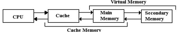
Figure: The Memory Hierarchy with Cache and Virtual Memory
We consider a multi-level memory system as having a faster primary memory and a slower secondary memory. In cache memory, the cache is the faster primary memory and the main memory is the secondary memory. We shall ignore virtual memory in this chapter.
In early computer designs, it
became common to add a single-level fast cache in order to improve performance
of the computer. This cache was placed
on a memory chip that was physically adjacent to the CPU chip. As later designs improved the circuit density
on the CPU chip, it became possible to add another cache that was physically on
the CPU chip. What we now have in the Intel
Pentium designs is a two-level cache, such as the following.
32 KB L1 cache (Level 1 cache with 16KB for
instructions and 16KB for data)
1MB L2 cache (Level 2 cache for both
data and instructions)
256 MB main memory
The argument for a two–level cache is based on the fact that, for a specific technology, smaller memories have a faster access time than larger memories. It is easy to show that a two–cache (32 KB and 1MB) has a much better effective access time than an equivalent monolithic cache of about 1MB.
Effective Access Time for Multilevel Memory
We have stated that the success of a multilevel memory system is due to the principle of locality. The measure of the effectiveness of this system is the hit ratio, reflected in the effective access time of the memory system.
We shall consider a multilevel memory system with primary and secondary memory. What we derive now is true for both cache memory and virtual memory systems. In this course, we shall use cache memory as an example. This could easily be applied to virtual memory.
In a standard memory system, an addressable item is referenced by its address. In a two level memory system, the primary memory is first checked for the address. If the addressed item is present in the primary memory, we have a hit, otherwise we have a miss. The hit ratio is defined as the number of hits divided by the total number of memory accesses; 0.0 £ h £ 1.0. Given a faster primary memory with an access time TP and a slower secondary memory with access time TS, we compute the effective access time as a function of the hit ratio. The applicable formula is TE = h·TP + (1.0 – h)·TS.
RULE: In this formula we must have TP < TS. This inequality defines the terms “primary”
and “secondary”. In this course TP
always refers to the cache memory.
For our first example, we
consider cache memory, with a fast
cache acting as a front-end for primary memory.
In this scenario, we speak of cache
hits and cache misses. The hit ratio is also called the cache hit ratio in these circumstances. For example, consider TP = 10
nanoseconds and TS = 80 nanoseconds.
The formula for effective access time becomes
TE = h·10 + (1.0 – h)·80. For sample values of hit ratio
Hit Ratio Access Time
0.5 45.0
0.9 17.0
0.99 10.7
The reason that cache memory works is that the principle of locality enables high values of the hit ratio; in fact h ³ 0.90 is a reasonable value. For this reason, a multi-level memory structure behaves almost as if it were a very large memory with the access time of the smaller and faster memory. Having come up with a technique for speeding up our large monolithic memory, we now investigate techniques that allow us to fabricate such a large main memory.
Memory As A
Collection of Chips
All modern computer memory is built from a collection of memory chips. The process of mapping an address space onto a number of smaller chips is called interleaving.
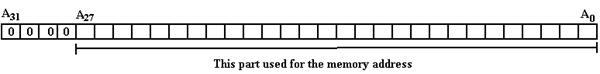
Suppose a computer with
byte-addressable memory, a 32–bit address space, and 256 MB
(228 bytes) of memory. Such a
computer is based on this author’s personal computer, with the memory size
altered to a power of 2 to make for an easier example. The addresses in the MAR can be viewed as 32–bit
unsigned integers, with high order bit A31 and low order bit A0. Ignoring issues of virtual addressing
(important for operating systems), we specify that only 28-bit addresses are
valid and thus a valid address has the following form.
The memory of all modern computers comprises a number of chips, which are combined to cover the range of acceptable addresses. Suppose, in our example, that the basic memory chips are 4MB chips. The 256 MB memory would be built from 64 chips and the address space divided as follows:
6 bits to select the memory chip as 26 = 64, and
22 bits to select the byte within
the chip as 222 = 4·220 = 4M.
The question is which bits select the chip and which are sent to the chip. Two options commonly used are high-order memory interleaving and low-order memory interleaving. We shall consider only low-order memory interleaving in which the low-order address bits are used to select the chip and the higher-order bits select the byte.
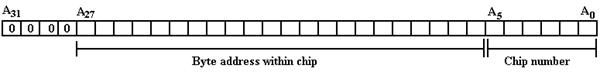
This low-order interleaving has a number of performance-related advantages. These are due to the fact that consecutive bytes are stored in different chips, thus byte 0 is in chip 0, byte 1 is in chip 1, etc. In our example
Chip 0 contains
bytes 0, 64, 128, 192, etc., and
Chip 1 contains bytes 1, 65, 129, 193, etc., and
Chip 63 contains bytes 63, 127, 191, 255, etc.
Suppose that the computer has a 128 bit data bus from the memory to the CPU. With the above low-order interleaved memory it would be possible to read or write sixteen bytes at a time, thus giving rise to a memory that is close to 16 times faster. Note that there are two constraints on the memory performance increase for such an arrangement.
1) The number of chips in the memory –
here it is 64.
2) The width of the data bus in bytes – here it is 16, the
lower number.
A design implementing such an address scheme might use a
6–to–64 decoder, or a pair of
3–to–8 decoders to select the chip and memory location within the chip. The next figure suggests the design with the
larger decoder.
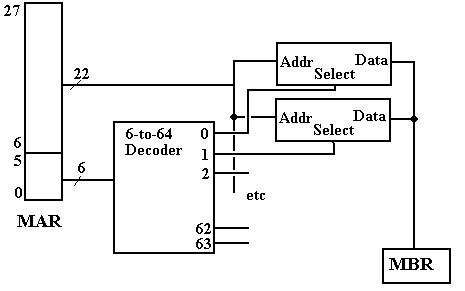
Figure: Partial Design of the Memory Unit
Note that each of the 64 4MB–chips receives the high order bits of the address. At most one of the 64 chips is active at a time. If there is a memory read or write operation active, then exactly one of the chips will be selected and the others will be inactive.
A Closer Look at the Memory “Chip”
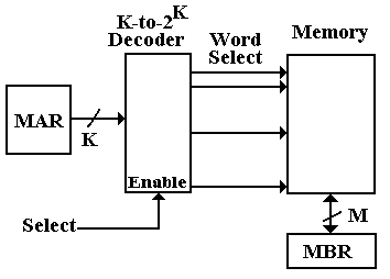
So far in our design, we have been able to reduce the problem of creating a 32–to–232 decoder to that of creating a 22–to–222 decoder. We have gained the speed advantage allowed by interleaving, but still have that decoder problem. We now investigate the next step in memory design, represented by the problem of creating a workable 4MB chip.
The answer that we shall use involves creating the chip with eight 4Mb (megabit) chips. The design used is reflected in the figures below.
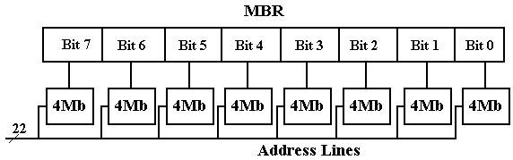
Figure: Eight Chips, each holding 4 megabits, making a 4MB “Chip”
There is an immediate advantage to having one chip represent only one bit in the MBR. This is due to the nature of chip failure. If one adds a ninth 4Mb chip to the mix, it is possible to create a simple parity memory in which single bit errors would be detected by the circuitry (not shown) that would feed the nine bits selected into the 8-bit memory buffer register.
A larger advantage is seen when we notice the decoder circuitry used in the 4Mb chip. It is logically equivalent to the 22–to–4194304 decoder that we have mentioned, but it is built using two 11–to–2048 decoders; these are at least not impossible to fabricate.
Think of the 4194304 (222) bits in the 4Mb chip as being arranged in a two dimensional array of 2048 rows (numbered 0 to 2047), each of 2048 columns (also numbered 0 to 2047). What we have can be shown in the figure below.
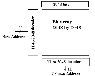
Figure: Memory with Row and Column Addresses
We now add one more feature, to be elaborated below, to our
design and suddenly we have a really fast DRAM chip. For ease of chip manufacture, we split the
22-bit address into an
11-bit row address and an 11-bit column address. This allows the chip to have only 11 address
pins, with two extra control (RAS and CAS – 14 total) rather than 22 address
pins with an additional select (23 total).
This makes the chip less expensive to manufacture.
We send the 11-bit row address first and then send the
11-bit column address. At first sight,
this may seem less efficient than sending 22 bits at a time, but it allows a
true speed-up. We merely add a 2048 SRAM
buffer onto the chip and when a row is selected, we transfer all 2048 bits in
that row to the buffer at one time. The
column select then selects from this faster memory used as an on-chip
buffer. Thus, our access time now has
two components:
1) The time to select a new row, and
2) The time to copy a selected bit from a row in the SRAM
buffer.
This design is the basis for all modern computer memory architectures.
SDRAM – Synchronous Dynamic Random Access Memory
As we mentioned above, the relative slowness of memory as compared to the CPU has long been a point of concern among computer designers. One recent development that is used to address this problem is SDRAM – synchronous dynamic access memory.
The standard memory
types we have discussed up to this point are
SRAM Static Random Access Memory
Typical access
time: 5 – 10 nanoseconds
Implemented with 6
transistors: costly and fairly large.
DRAM Dynamic Random Access Memory
Typical access
time: 50 – 70 nanoseconds
Implemented with
one capacitor and one transistor: small and cheap.
In a way, the desirable approach would be to make the entire memory to be SRAM. Such a memory would be about as fast as possible, but would suffer from a number of setbacks, including very large cost (given current economics a 256 MB memory might cost in excess of $20,000) and unwieldy size. The current practice, which leads to feasible designs, is to use large amounts of DRAM for memory. This leads to an obvious difficulty.
1) The access time on DRAM is almost never less than 50 nanoseconds.
2) The clock time on
a moderately fast (2.5 GHz) CPU is 0.4 nanoseconds,
125 times faster than the
DRAM.
The problem that arises from this speed mismatch is often called the “Von Neumann Bottleneck” – memory cannot supply the CPU at a sufficient data rate. Fortunately there have been a number of developments that have alleviated this problem. We have already discussed the idea of cache memory, in which a large memory with a 50 nanosecond access time can be coupled with a small memory with a 10 nanosecond access time and function as if it were a large memory with a 10.4 nanosecond access time. We always want faster.
The next development that we shall discuss is synchronous dynamic access memory, SDRAM for short. Although we have not mentioned it, earlier memory was asynchronous, in that the memory speed was not related to any external speed. In SDRAM, the memory is synchronized to the system bus and can deliver data at the bus speed. The earlier SDRAM chips could deliver one data item for every clock pulse; later designs called DDR SDRAM (for Double Data Rate SDRAM) can deliver two data items per clock pulse.
Modern computer designs, in an effort to avoid the Von Neumann bottleneck, use several tricks, including multi-level caches and DDR SDRAM main memory.
As an example, we quote from the Dell Dimension 4700 advertisement of July 21, 2004. The chip has two 16 KB L1 caches (an Instruction Cache and a Data Cache), 1MB L2 cache, and 512 MB of DDR SDRAM that operates with a 400 MHz bus (800 M transfers/sec) with 64 data lines – 8 bytes at a time, for a data rate of 6.4 GB/sec.
The main difference between level 1 (L1) cache and level 2 (L2) cache is that the L1 cache is on the CPU chip, while the L2 cache generally is on a different chip. For example, the IBM S390/G5 chip has 256 KB of L1 cache on the CPU chip and 4MB of L2 cache. It is likely that the existence of two (or more) levels of cache, rather than one large L1 cache, is due to two aspects of area constraints: area on the CPU chip that can be allocated to the L1 cache and the fact that larger SRAM memories tend to be slower than the smaller ones.
L1 cache memory is uniformly implemented as SRAM (Static RAM), while L2 cache memory may be either SRAM or SDRAM.
The SDRAM chip uses a number of tricks to deliver data at an acceptable rate. As an example, let’s consider a modern SDRAM chip capable of supporting a DDR data bus. In order to appreciate the SDRAM chip, we must begin with simpler chips and work up.
We begin with noting an approach that actually imposes a performance hit – address multiplexing. Consider an NTE2164, a typical 64Kb chip. With 64K of addressable units, we would expect 16 address lines, as 64K = 216. In stead we find 8 address lines and two additional control lines
![]() Row Address
Strobe (Active Low)
Row Address
Strobe (Active Low)
![]() Column
Address Strobe (Active Low)
Column
Address Strobe (Active Low)
Here is how it works. Recalling that 64K = 216 = 28 · 28 = 256 · 256, we organize the memory as a 256-by-256 square array. Every item in the memory is uniquely identified by two addresses – its row address and its column address.
Here is the way that the 8-bit address is interpreted.
|
|
|
Action |
|
0 |
0 |
An error – this had better not happen. |
|
0 |
1 |
It is a row address (say the high order 8-bits of the 16-bit address) |
|
1 |
0 |
It is a column address (say the low order 8-bits of the 16-bit address) |
|
1 |
1 |
It is ignored. |
Here is that way that
the NTE2164 would be addressed.
1) Assert
![]() = 0 and place the A15
to A8 on the 8-bit address bus.
= 0 and place the A15
to A8 on the 8-bit address bus.
2) Assert
![]() = 0 and place A7
to A0 on the 8-bit address bus.
= 0 and place A7
to A0 on the 8-bit address bus.
There are two equivalent design goals for such a design.
1) To minimize the
number of pins on the memory chip. We
have two options:
8 address pins,
RAS, and CAS (10 pins), or
16 address pins
and an Address Valid pin (17 pins).
2) To minimize the
number of address-related lines on the data bus.
The same numbers
apply here: 10 vs. 17.
With this design in mind, we are able to consider the next step in memory speed-up. It is called Fast-Page Mode DRAM, or FPM–DRAM.
Fast-Page Mode DRAM implements page mode, an improvement on conventional DRAM in which the row-address is held constant and data from multiple columns is read from the sense amplifiers. The data held in the sense amps form an “open page” that can be accessed relatively quickly. This speeds up successive accesses to the same row of the DRAM core.
The move from FPM–DRAM to SDRAM is logically just making the DRAM interface synchronous to the data bus in being controlled by a clock signal propagated on that bus. The design issues are now how to create a memory chip that can respond sufficiently fast. The underlying architecture of the SDRAM core is the same as in a conventional DRAM. SDRAM transfers data at one edge of the clock, usually the leading edge.
Double Data Rate SDRAM (DDR–SDRAM) doubles the bandwidth available from SDRAM by transferring data at both edges of the clock.
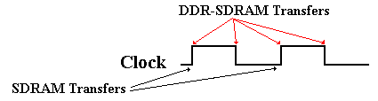
Figure: DDR-SDRAM Transfers Twice as Fast
So far, we have used a SRAM memory as a L1 cache to speed up effective memory access time and used Fast Page Mode DRAM to allow quick access to an entire row from the DRAM chip. We continue to be plagued with the problem of making the DRAM chip faster. If we are to use the chip as a DDR-SDRAM, we must speed it up quite a bit.
Modern DRAM designs are increasing the amount of SRAM on the DRAM die. In most cases a memory system will have at least 8KB of SRAM on each DRAM chip, thus leading to the possibility of data transfers at SRAM speeds.
We are now faced with two measures: latency and bandwidth.
Latency is the amount of time for the memory to provide the
first element of a block
of contiguous data.
Bandwidth is the rate at which the memory can deliver data once
the row address
has been accepted.
One can increase the bandwidth of memory by making the data bus “wider” – that is able to transfer more data bits at a time. It turns out that the optimal size is half that of a cache line in the L2 cache. Now – what is a cache line?
In order to understand the concept of a cache line, we must return to our discussion of cache memory. What happens when there is a cache miss on a memory read? The referenced byte must be retrieved from main memory. Efficiency is improved by retrieving not only the byte that is requested, but also a number of nearby bytes.
Cache memory is organized into cache lines. Suppose that we have a L2 cache with a cache line size of 16 bytes. Data would be transferred into the L2 cache in units of 8 bytes.
Suppose that the byte with address 0x124A is requested and found not to be in the L2 cache. A cache line in the L2 cache would be filled with the 16 bytes with addresses ranging from 0x1240 through 0x124F. This might be done in two transfers of 8 bytes each.
Now suppose that the memory is 8-way interleaved, with chips that could be numbered 0 through 7, so that chip 0 had bytes 1240 and 1248, chip 1 had byte 1241 and 1249, etc. Also we suppose that each of the 8 memory chips has a dedicated set of 8 data lines, for a total bus width of 64 bits. We fill the cache line as follows.
1) Assert the address
on the address lines and wait for the memory latency.
2) Transfer
the first set of 8 bytes at the same time, using the full bus speed.
3) Transfer
the next set of 8 bytes at the same time, using the full bus speed.
The DDR–SDRAM would then transfer 8 bytes on each clock edge, for a total of 16 bytes per clock pulse. A 400 MHz synchronous bus would then transfer data at a rate of 16 bytes · 400 M/Sec or 6.4 GB/Sec.
We close this part of
the discussion by examining some specifications of a memory chip that as of
July 2004 seemed to be state-of-the-art.
This is the Micron DDR2 SDRAM in 3 models
MT46H64M4 64 MEG x 4
MT47H32M8 32 MEG x 8
MT47H16M16 16 MEG x 16
Each of these chips can be synchronized with one of two bus clock times.
5 nanoseconds for
a 200 MHz bus, or 400 M transfers per second at DDR.
3.75 nanoseconds for a 266.7 MHz bus, or 533 M transfers per
second at DDR.
Each of the chips contains 256 Mb, internally configured as a 4-bank DRAM. Depending on the chip option, this can be 4 banks of 4, 8, or 16-bit entries. Call this number N. A single read or write access to the chip effectively consists of a single 4N-bit-wide. one-clock-cycle data transfer at the DRAM core and four corresponding N-bit-wide transfers at the I/O pins.
A modern data bus might
be 64 bits wide, thus capable of transferring 8 bytes at a time. The bandwidths of a bus using the above
technologies would be either
8 bytes/transfer· 400
M transfers/sec = 3200 MB/Sec = 3.2 GB/sec, or
8 bytes/transfer· 533
M transfers/sec = 4264 MB/Sec = 4.3 GB/sec.
At such data rates, we have largely removed the memory bottleneck.
Gulliver’s Travels
and “Big-Endian” vs. “Little-Endian”
The author of these notes has been told repeatedly of the literary antecedents of the terms “big-endian” and “little-endian” as applied to byte ordering in computers. In a fit of scholarship, he decided to find the original quote. Here it is, taken from Chapter IV of Part I (A Voyage to Lilliput) of Gulliver’s Travels by Jonathan Swift, published October 28, 1726.
The edition consulted for these notes was published in 1958 by Random House, Inc. as a part of its “Modern Library Books” collection. The LC Catalog Number is 58-6364.
The story of “big-endian” vs. “little-endian” is described in the form on a conversation between Gulliver and a Lilliputian named Reldresal, the Principal Secretary of Private Affairs to the Emperor of Lilliput. Reldresal is presenting a history of a number of struggles in Lilliput, when he moves from one difficulty to another. The following quote preserves the unusual capitalization and punctuation found in the source material.
“Now, in the midst of these intestine Disquiets, we are threatened with an Invasion from the Island of Blefuscu, which is the other great Empire of the Universe, almost as large and powerful as this of his majesty. ….
[The two great Empires of Lilliput and Blefuscu] have, as I was going to tell you, been engaged in a most obstinate War for six and thirty Moons past. It began upon the following Occasion. It is allowed on all Hands, that the primitive Way of breaking Eggs before we eat them, was upon the larger End: But his present Majesty’s Grand-father, while he was a Boy, going to eat an Egg, and breaking it according to the ancient Practice, happened to cut one of his Fingers. Whereupon the Emperor his Father, published an Edict, commanding all his Subjects, upon great Penalties, to break the smaller End of their Eggs. The People so highly resented this Law, that our Histories tell us, there have been six Rebellions raised on that Account; wherein one Emperor lost his Life, and another his Crown. These civil Commotions were constantly fomented by the Monarchs of Blefuscu; and when they were quelled, the Exiles always fled for Refuge to that Empire. It is computed, that eleven Thousand Persons have, at several Times, suffered Death, rather than submit to break their Eggs at the smaller end. Many hundred large Volumes have been published upon this Controversy: But the Books of the Big-Endians have been long forbidden, and the whole Party rendered incapable by Law of holding Employments.”
Jonathan Swift was born in