Example:
Interpretation of a Digital Circuit
Here
is a sample problem, taken from the textbook The Essentials of Computer
Organization and Architecture by Linda Null and Julia Lobur.
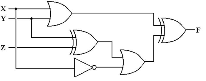
The task is to represent this
circuit by both a Boolean expression and a
Truth Table. Admittedly, this will prove
to be a silly circuit.
Interpreting
a Digital Circuit: Step 1
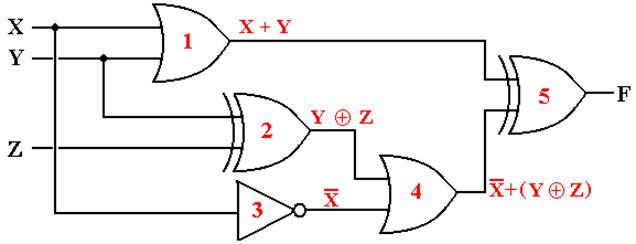
Label
the circuit elements (I have chosen to use numbers) and label the output
of each element. Note that we are slowly
building a Boolean expression.
The
outputs of each gate are as follows:
The output of gate 1 is (X + Y),
The output
of gate 2 is (Y Å Z),
The output of gate 3 is X’,
The output of gate 4 is X’ + (Y Å Z), and
The output of gate 5 is (X + Y) Å [X’ + (Y Å Z)]
Interpreting
a Digital Circuit: Step 2
For
a circuit of this complexity, the best next step is to make a Truth Table.
|
X |
Y |
Z |
X + Y |
(Y Å Z) |
X’ |
X’ + (Y Å Z) |
(X + Y) Å [X’+(Y Å Z)] |
|
0 |
0 |
0 |
0 |
0 |
1 |
1 |
1 |
|
0 |
0 |
1 |
0 |
1 |
1 |
1 |
1 |
|
0 |
1 |
0 |
1 |
1 |
1 |
1 |
0 |
|
0 |
1 |
1 |
1 |
0 |
1 |
1 |
0 |
|
1 |
0 |
0 |
1 |
0 |
0 |
0 |
1 |
|
1 |
0 |
1 |
1 |
1 |
0 |
1 |
0 |
|
1 |
1 |
0 |
1 |
1 |
0 |
1 |
0 |
|
1 |
1 |
1 |
1 |
0 |
0 |
0 |
1 |
We have now solved the
problem. I want to continue and produce
a simpler expression.
(At least I think that it is simpler).
Interpreting
a Digital Circuit: Step 3
Present
the truth table without the intermediate expressions. Use the standard rules to convert the truth
table to either Canonical SOP or Canonical POS.
We do both.
|
X |
Y |
Z |
F(X, Y, Z) |
|
0 |
0 |
0 |
1 |
|
0 |
0 |
1 |
1 |
|
0 |
1 |
0 |
0 |
|
0 |
1 |
1 |
0 |
|
1 |
0 |
0 |
1 |
|
1 |
0 |
1 |
0 |
|
1 |
1 |
0 |
0 |
|
1 |
1 |
1 |
1 |
SOP: F(X, Y, Z) = X’·Y’·Z’ + X’·Y’·Z + X·Y’·Z’ + X·Y·Z
0
0 0 0 0 1 1 0 0 1
1 1
POS: F(X,
Y, Z) = (X + Y’ + Z) · (X + Y’ + Z’) · (X’ + Y + Z’) · (X’ + Y’ + Z)
0
1 0 0 1 1 1 0 1 1 1 0
Interpreting
a Digital Circuit: Step 4
SOP:
F(X,
Y, Z) = X’·Y’·Z’ + X’·Y’·Z + X’·Y’·Z’ + X·Y’·Z’ + X·Y·Z
= X’·Y’·(Z’ + Z) + (X + X’)·Y’·Z’ + X·Y·Z
= X’·Y’ + Y’·Z’ + X·Y·Z
POS:
F(X, Y, Z) = (X + Y’ + Z) · (X + Y’ + Z’) · (X’ + Y + Z’)
· (X’ + Y’ + Z) · (X + Y’ + Z)
= (X + Y’) · (X’ + Y + Z’)· (Y’ + Z)
One
can also write
F(X, Y, Z) = S(0, 1, 4, 7)
F(X, Y, Z) = P(2, 3, 5, 6)
This
is about as simple as I can make these expressions.
Building a
Digital Circuit for a Boolean Expression
We
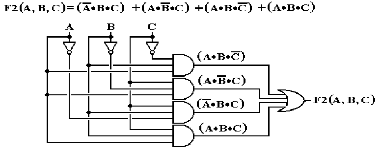
take as examples two representations of the same Boolean expression.

Sum of Products
SOP One OR gate connecting the output of a
number of AND gates.
Building a
Digital Circuit (Part 2)

Product of Sums
POS One AND gate connecting the output of a
number of OR gates.
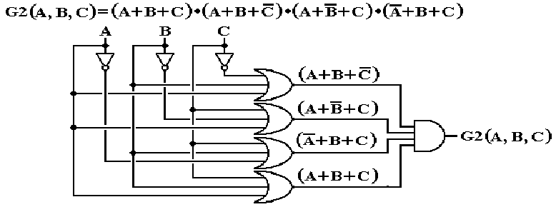
There are simpler Boolean
expressions that are equivalent to both F2 and G2,
which are equivalent to each other. We
study simplification later.
Stylistics
There
are very few issues involved in drawing a digital implementation of
a Boolean circuit. The basic issue is
DRAWING NEATLY.
My
style of having the inputs at the top, with each input immediately feeding a
NOT gate, if necessary, is only a convention.
It helps me minimize the clutter in a drawing. The student may adopt any style that is easy
to understand.
Big Gates
This
style will ask for gates with a large number of inputs.
Here is an 8–input AND fabricated from three 4–input AND gates.
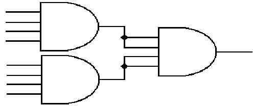
The
AND gate on the right could also be a 2–input or 3–input gate.